With the advent of the Fourth Industrial Revolution (Industry 4.0), industrial automation is evolving from simple mechanical substitution toward highly integrated, intelligent systems capable of real-time sensing, communication, and decision-making. As the “nervous system” of these platforms, the performance and reliability of Printed Circuit Boards (PCBs) play a decisive role in factory efficiency, operational continuity, and production safety.
Unlike consumer electronics—where miniaturization and aesthetics dominate—industrial PCBs prioritize long-term stability, extreme-environment reliability, and complex signal integrity. As a hybrid online–offline PCB manufacturing and assembly service provider, NextPCB leverages its expertise in material engineering and precision manufacturing to deliver end-to-end solutions—from prototyping to mass production—for industrial control systems, robotics, sensors, and energy management applications.
1. Core Technical Challenges for PCBs in Industrial Automation Environments
Industrial environments are inherently harsh. PCBs deployed on factory floors must withstand high temperatures, high voltage, strong electromagnetic interference (EMI), mechanical vibration, and chemical exposure. These conditions demand exceptional robustness and design redundancy at both the layout and manufacturing stages.
1.1 Thermal Management and Power Load
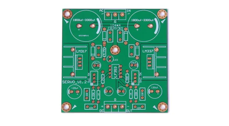
Industrial motor drives and power modules often handle extremely high current loads, frequently exceeding 100 A. According to Joule's law (P = I2R), even minimal resistance in copper traces can generate substantial heat under high current conditions. If this heat is not dissipated efficiently, it can lead to substrate delamination, solder joint fatigue, or catastrophic component failure.
From an engineering standpoint, heavy copper PCBs and metal-core PCBs (MCPCB / copper-core boards) are widely adopted in power electronics and motor control applications due to their superior current-carrying capacity and thermal conductivity.
1.2 Mechanical Stress and Vibration Resistance
PCBs installed in robotic joints, CNC machines, or automated production lines are subjected to continuous vibration and cyclic mechanical stress. These stresses can induce fatigue cracks in BGA solder joints or cause structural failures in vias along the Z-axis.
To mitigate such risks, industrial PCB designs often incorporate reinforcement ribs, underfill materials, filled vias, and optimized lamination stack-ups, all of which significantly enhance mechanical integrity and service life.
2. NextPCB's Manufacturing Capabilities for Industrial-Grade Requirements
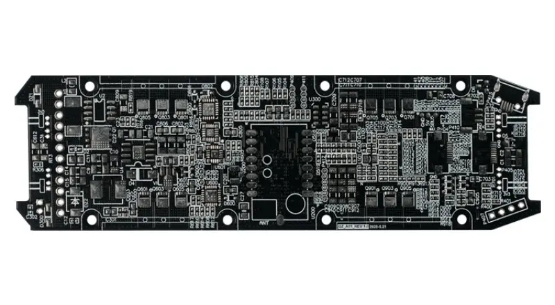
NextPCB operates multiple self-owned fabrication plants and two major assembly facilities in China, supported by 36 Siemens automated SMT production lines. This infrastructure enables a fully closed-loop manufacturing workflow, covering prototypes through high-volume production. The company demonstrates strong capabilities in multilayer boards, HDI, heavy copper, and metal-core PCBs.
>>> Advanced PCB Capabilities | HDI & 32+ Layers | NextPCB
>>> PCB Capabilities - NextPCB
2.1 Key Manufacturing Specifications
To meet the demands of high-integration and high-reliability industrial control systems, NextPCB supports up to 32-layer PCBs and complex HDI architectures (from 1+N+1 up to 3+N+3 and any-layer designs).
| Technical Parameter |
Standard Capability |
Advanced Capability |
Industrial Value |
| Layer Count |
1–20 layers |
Up to 32 layers (40+ possible) |
Enables complex PLC and master control integration |
| Min. Trace / Space |
3.5 / 3.5 mil |
2.5 / 2.5 mil |
Higher routing density for compact designs |
| Min. Mechanical Drill |
0.20 mm |
0.15 mm |
Optimized BGA fan-out and HDI interconnect |
| HDI Structure |
1–3 step |
Any-layer HDI |
Maximizes functionality in limited space |
2.2 Heavy Copper Manufacturing and Advanced Thermal Solutions
For power electronics and motor control systems, NextPCB provides heavy copper and metal-core PCB solutions. In high local heat-density scenarios, advanced techniques such as copper coins, embedded copper slugs, and pedestal structures are employed to minimize thermal bottlenecks and enhance heat transfer efficiency.
- Heavy Copper Support: Officially supports copper thicknesses up to 10 oz, significantly improving current capacity and thermal dissipation.
- Metal-Core PCBs: Aluminum and copper substrates provide a more direct thermal conduction path than conventional thermal vias, ideal for high-power industrial modules.
3. Protective Coating and Assembly Services for Harsh Environments
Industrial PCBs are frequently exposed to humidity, salt spray, corrosive gases, and conductive dust, all of which can drastically reduce operational lifespan. NextPCB's conformal coating and assembly services offer a comprehensive protective barrier against these threats.
3.1 Automated Selective Conformal Coating
NextPCB supports multiple coating methods, including masking, brushing, dipping, and selective spraying. Automated selective coating systems with programmable robotic nozzles precisely avoid sensitive areas such as connectors and switches while ensuring consistent coverage.
Film Thickness Control: Dry film thickness is typically maintained within 1–5 mil (≥20 μm), meeting industry standards for industrial protection.
3.2 Coating Material Selection
- Silicone Resin (SR): Excellent flexibility and thermal endurance (-40°C to 200°C), commonly used in robotic controllers.
- Polyurethane (UR): Superior chemical resistance and abrasion durability, ideal for chemical processing equipment.
>>> PCB Capabilities Supporting Industrial Automation
Heavy Copper & Thermal Management Solutions
Heavy copper PCBs, metal-core substrates, and embedded copper structures designed to handle high current loads, power electronics, and thermal-intensive industrial applications.
See Industrial PCB Capabilities
Turnkey PCB Assembly for Industrial Systems
End-to-end component sourcing, SMT, THT, conformal coating, and IPC Class 3 assembly services optimized for industrial control, robotics, and automation equipment.
View Industrial Assembly Services
4. Industrial Automation Applications and Customized Solutions
- Industrial Control & PLC Systems: Multilayer designs with controlled impedance (±5%) ensure microsecond-level response across large I/O counts.
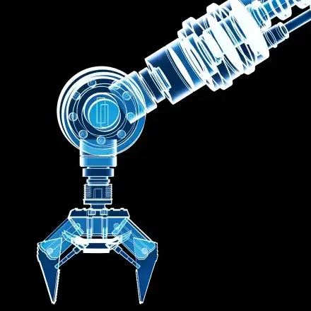
- Robotics & Motion Control: Rigid-flex PCBs eliminate cable interconnect failures, improving reliability in dynamic environments.
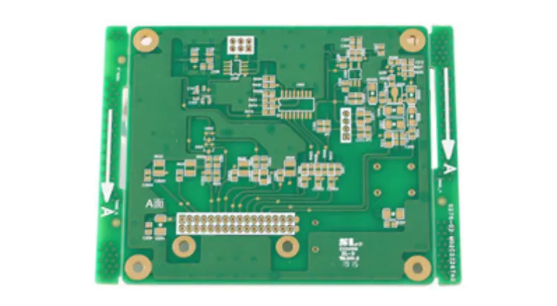
- Smart Sensors & IIoT Devices: HDI technology and ultra-small component assembly (01005 support) enable compact sensor and communication integration.
5. Quality Management Systems: Reliability as a Safety Boundary
In industrial automation, quality is not merely a performance metric—it is a safety guarantee.
- IATF 16949:2016 Certification: Ensures defect prevention, process consistency, and full lifecycle traceability—critical for high-reliability industrial and automotive-adjacent applications.
- IPC Class 3 Assembly: Supports the highest assembly standard for mission-critical industrial and medical electronics, ensuring resilience under extreme vibration and thermal shock.
- Browse NextPCB Quality Certifications and Test Reports
6. Digital Integration Services in the Industry 4.0 Era
Aligned with Industry 4.0 principles, NextPCB integrates digital supply chain systems and MES platforms to provide end-to-end traceability—from component sourcing to final inspection.
7. Addressing Industry Pain Points: Delivery and Scalability Advantages
Industrial automation projects often require high-mix, low-volume development cycles. NextPCB addresses this challenge with rapid prototyping and scalable production.
- 24-Hour Quick Turn Prototyping: Enables engineers to quickly validate thermal and signal designs during R&D.
- Seamless Transition to Mass Production: Backed by 36 Siemens SMT lines, ensuring DFM/DFA consistency from prototype to volume manufacturing.
Get a Prototype Quote in Minutes Inquire About Volume Assembly
8. Conclusion
In the complex landscape of industrial automation, NextPCB has spent over 15 years building a comprehensive service ecosystem that combines advanced manufacturing (10 oz heavy copper, embedded copper structures), full-spectrum environmental protection (automated selective conformal coating), rigorous quality assurance (IATF 16949, IPC Class 3), and a digitally integrated supply chain.
Through stable engineering execution and long-term manufacturing reliability, NextPCB has become a trusted partner for industrial customers seeking high-complexity PCB manufacturing and assembly solutions in the Industry 4.0 era.
Related PCB Application Industries

 NextPCB Capabilities
 PCB Assembly
 Layer Buildup
 SMD-Stencils
 PCB Design-Aid & Layout
 Mechanics
 Quality
 Drills & Throughplating
 Factory & Certificate
 PCB Assembly Factory Show
Certificate
PCB Assembly Factory Show
Certificate
 NextPCB Capabilities
 PCB Assembly
 Layer Buildup
 SMD-Stencils
 PCB Design-Aid & Layout
 Mechanics
 Surface
 Quality
 Drills & Throughplating
 Factory & Certificate