Support Team
Feedback:
support@nextpcb.com
Security & Surveillance PCB & PCBA
PCBs for cameras, recorders and sensors
For cameras, recorders, access control and sensors: HDI, flex, metal core and assembly with flashing.
Used in IP cameras, NVR/DVR recorders, access control, alarm panels and sensors.
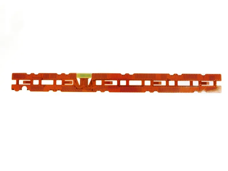
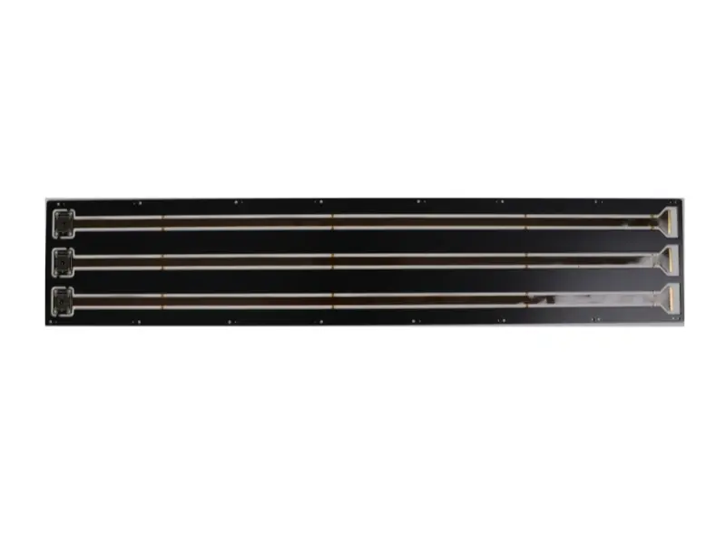
HDI up to 3 steps, plus flex and rigid-flex for module links.
High-Tg FR-4, thermal shock testing and selective conformal coating.
PCB, parts sourcing, SMT, firmware flashing and functional test in one place.
Pick by where the board sits: camera, lighting or recorder.


Best values for each board type.
| HDI and signal | |
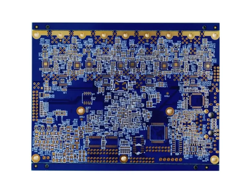
| HDI structures | 1–3 steps: 1+N+1, 2+N+2, 3+N+3; blind and buried vias, stacked and staggered vias |
| Min. laser via | 0.075 mm (0.10 mm typical) |
| Min. mechanical drill | 0.15 mm |
| Min. trace / space | 3.5/3.5 mil standard; HDI as fine as 2/2 mil |
| Impedance control | ±10% standard, ±5% on request |
| Flex and rigid-flex | |
| Flex layers | 1–6, polyimide base |
| Flex min. trace / space | 2/2 mil |
| Stiffeners and contacts | FR-4, polyimide or steel stiffeners; gold finger and ZIF |
| Rigid-flex | Rigid part 2–32 layers |
| Metal core and materials | |
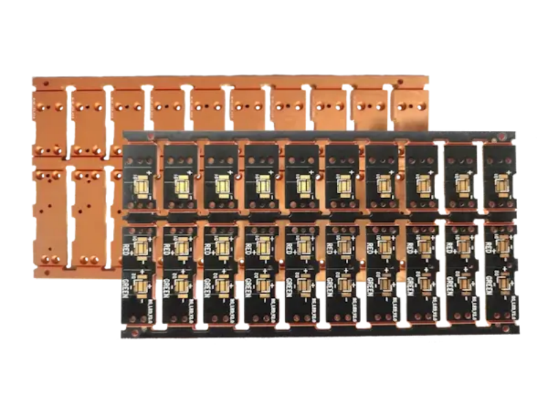
| Metal core bases | Aluminum, copper, iron, stainless steel; single, double and multilayer |
| Copper base | 1–2 layers, 1/2/3 W/mK, 0.8–3.0 mm |
| Tg | 130, 150 and 170 °C; high-Tg is 170 °C and above |
| Board thickness | 0.6–3.2 mm |
| Hole copper | Class 2: 18 µm min, 20 µm avg · Class 3: 20 µm min, 25 µm avg |
| Panels, finish and test | |
| Panelizing | V-cut (30°, 45°, 60°; 0.25–0.5 mm web, ±0.1 mm), stamp holes, spaced panels |
| Surface finish | HASL (lead-free or leaded), ENIG, ENEPIG, immersion silver, OSP, hard gold |
| Electrical test | Flying probe with no point limit; fixture test under 14,000 points |
| Reports | Shipping, microsection, impedance test |
Values are the best for each board type and do not always combine in one design. Planning impedance? Try the stack-up tool. Full tables: Advanced PCB · Standard PCB
From SMT to firmware, inspection and coating.

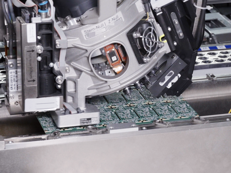
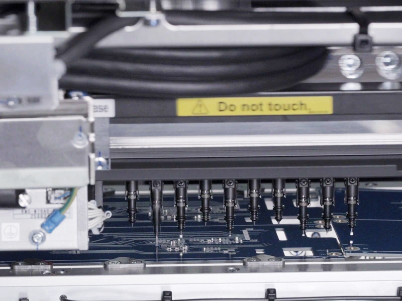
Multi-nozzle placement head mounting components on a PCB panel.

SIPLACE placement head working on a PCB panel.
| Boards and parts | |
| Board size / thickness | 50 × 50 mm to 510 × 460 mm / 0.2–5 mm |
| Component size / height | 01005 to 45 × 98 mm / up to 25 mm |
| Soldering | |
| Reflow | 10–12 zone air reflow and nitrogen reflow |
| Through-hole | Selective wave soldering, wave soldering, hand soldering |
| Press-fit | Hole tolerance ±0.05 mm |
| Inspection and test | |
| Inspection | 2D/3D SPI, AOI, 2D/3D X-ray for BGA balls and QFN thermal pads |
| Firmware flashing | Hex, bin and elf files; SOP written at first article |
| Functional test | UART, I2C, SPI; USB, HDMI and Ethernet ports; memory, voltage, current; LED, button and sensor response |
| Finish and scale | |
| Conformal coating | Automated selective spray, infrared cure |
| Added processes | Potting, aging |
| SMT/PCBA site | 15,000 m², 50 SIPLACE (Siemens) E-series lines |
| Order quantity | From 1 piece, up to large batches |
Learn more: assembly capabilities · PCB assembly services · functional testing
What we support. Need salt spray, damp heat or HAST? Send your test plan and engineers will tell you what we can arrange.
Thermal shock and T260/T288 time-to-delamination testing.
Electric strength (750 V/mil), arc resistance (over 60 s), moisture and insulation resistance.
Ionic contamination testing controls residue that can cause leakage.
Automated selective spray with infrared cure. Send coating type and keep-out areas.
Typical times for standard prototype orders.
| PCB build time | |
| 1–2 layers | As fast as 24 hours |
| 4 layers | 1–2 days |
| 6 layers and above | 2–3 days |
| HDI, flex, metal core | Confirmed at quotation |
| PCB assembly | |
| Express | 24 hours once all parts are ready |
| Standard | 5–7 working days with parts from HQ Online |
| Order quantity | From 1 piece |
Volume PCBs are built at a site with 100,000 m² monthly capacity, and our SMT lines place over 98 million components a day. Try HQDFM · Get a PCB quote · Get a PCBA quote
Know where every part and board came from.
Components come through HQ Online from original manufacturers and authorized distributors, with incoming inspection.
Send some or all parts, or let us source. Your own programmers and test cables are welcome.
Our MES supports laser-marked or printed barcodes and QR codes, with batch date codes.
Third-party RoHS, REACH and PFAS reports for lead-free HASL, ENIG and OSP boards.
Quality systems and test reports behind every board.
You
Upload Gerber files with stack-up, impedance and finish. Add BOM, firmware and test needs for assembly.
NextPCB
Automated DFM pre-review in about a minute, an engineer within 30 minutes.
NextPCB
Sourcing, SMT, firmware flashing and functional test. Engineers write the flashing and test SOP at first article.
Together
On reorders with unchanged files, engineers reuse the earlier data. Changes are noted at reorder.
Camera main boards often use multilayer or HDI boards, module links use flex or rigid-flex, and infrared lighting boards use metal core. We build all of these. Send your stack-up and engineers will confirm it.
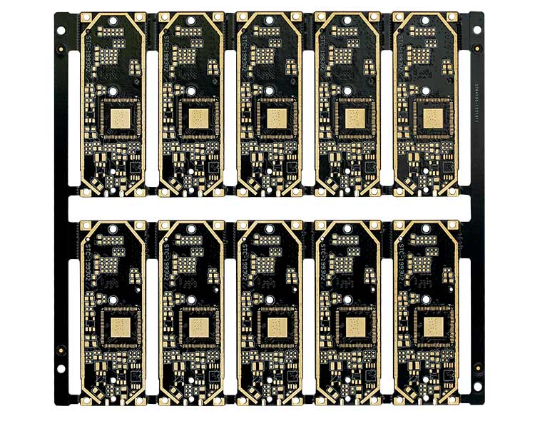
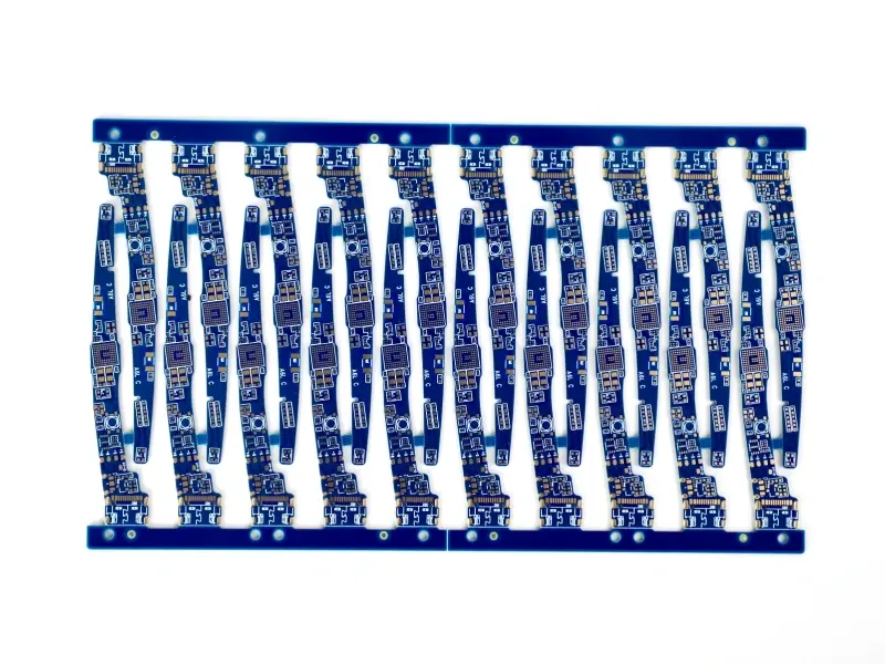
HDI goes up to 3 steps (1+N+1, 2+N+2 and 3+N+3) with laser vias down to 0.075 mm, and flex boards support 2/2 mil trace and space. Very small sensor boards ship in panels with V-cut or stamp-hole panelizing. Send your outline so engineers can confirm the panel.
Yes. Impedance tolerance is ±10% as standard and ±5% on request. Functional test includes USB, HDMI and Ethernet port checks. Send your stack-up and required impedances for review.
Metal core boards use an aluminum, copper, iron or stainless steel base, and can be single-sided, double-sided or multilayer. Copper-base boards are 1–2 layers with 1, 2 or 3 W/mK and 0.8–3.0 mm thickness.
We support thermal shock, T260 and T288 time-to-delamination, electric strength, arc resistance, moisture and insulation resistance, peel strength and ionic contamination testing. Salt spray, damp heat and HAST are not on our standard list. Send your test plan and engineers will tell you what can be arranged.
High-Tg FR-4 (Tg 170 °C or higher) resists delamination and thermal shock better than standard grades. Finishes include ENIG, OSP, immersion silver, ENEPIG, HASL (lead-free or leaded) and hard gold. Add conformal coating if your enclosure needs it, and send the coating type and keep-out areas.
Yes. Conformal coating uses automated selective spraying with infrared curing. Potting and aging are offered as added processes. Send the coating type, thickness and keep-out areas, plus your aging requirements, for engineer review.
Yes. We flash .hex, .bin and .elf firmware and run functional tests: UART, I2C and SPI communication, USB, HDMI and Ethernet port checks, memory read and write, voltage and current, and LED, button and sensor response. Engineers write the flashing and test SOP at first article, and volume runs follow it.
Components come through HQ Online from original manufacturers and authorized distributors, and incoming parts are inspected and logged. Parts are not substituted without your written confirmation. Our MES supports laser-marked or printed barcodes and QR codes on boards, with batch date codes.
Yes. We support turnkey, consigned and mixed builds. You can send some or all parts, plus your own programmer, development board or test cables. Engineers debug the first article with you (about 0.5–1 hour), then write the flashing and test SOP before volume.
Parts or boards with pre-bake requirements can be baked in precision ovens before assembly, and shipments can use moisture-proof sealed bags with humidity cards. Tell engineers about moisture-sensitive or large BGA parts when you quote.
When your files do not change, engineers reuse the earlier engineering data, so stack-up, impedance and artwork stay the same. If a file changes, note it in the reorder and engineers rebuild the data. Flashing and test orders are verified at first article before volume.
Prototypes ship as fast as 24 hours for 1–2 layers, 1–2 days for 4 layers and 2–3 days for 6 layers and above. HDI, flex and metal core timing is confirmed at quotation. The minimum order is 1 piece for PCB and PCBA. Volume PCBs are built at a site with 100,000 m² monthly capacity.
Send photos, the lot or date code and the failure conditions. Engineers can check with microsection, X-ray and ionic contamination testing. X-ray covers BGA solder balls, bridging and QFN pad voids, and microsection shows hole copper, plating and layer defects. Findings are reviewed with you before any corrective action.
EMC, EMI and IP rating belong to the whole product and are tested on the finished device. On the PCB side, upload your files to HQDFM, our free design check, and engineers review impedance traces, ground planes and hole-to-copper clearances. Conformal coating and potting can support ingress protection. FCC/CE certification assistance is also offered; ask your engineer for scope.
ISO 9001 and ISO 14001 cover our PCB and PCBA sites. UL 94V-0 laminates are available (UL file E469747). Third-party RoHS, REACH and PFAS reports are available for lead-free HASL, ENIG and OSP boards, and fabrication and assembly go up to IPC Class 3.
Upload Gerber and BOM files for an instant quote, or send your requirements to our engineers first. NDAs are available on request. Not ready to quote? Check your design with free HQDFM first.
Technical hotline +86 755 8364 3663 (24/7) · support@nextpcb.com
Support in English · Team time zone: China Standard Time (UTC+8)
PCB is the abbreviation of the...