Contact Us
Blog / PCB Gold Fingers: Design & Manufacturing Guide

PCB Gold Fingers: Design & Manufacturing Guide

Posted: February, 2026 Writer: NextPCB Content Team Share: NEXTPCB Official youtube NEXTPCB Official Facefook NEXTPCB Official Twitter NEXTPCB Official Instagram NEXTPCB Official Linkedin NEXTPCB Official Tiktok NEXTPCB Official Bksy

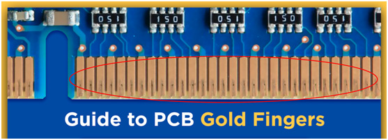
In the world of printed circuit board (PCB) interconnection, durability and signal integrity are paramount. Gold fingers are the gold-plated columns found along the connecting edges of printed circuit boards (PCBs). They serve as the critical connecting interface between a secondary PCB (like a graphics card or RAM stick) and the computer's motherboard.

For engineers and procurement specialists looking for reliable PCB manufacturing, understanding the specifications of gold fingers is essential to prevent connection failures and signal loss.

  1. Table of Contents
  2. What are PCB Gold Fingers?
  3. Material Science: Hard Gold vs. ENIG
  4. Key Applications and Usage
  5. Critical Design Specifications (IPC Standards)
  6. The Manufacturing Process: Plating & Beveling
  7. DFM Tips for High-Quality PCB Assembly
  8. FAQ: Common Questions About Gold Fingers

PCB Gold Fingers Example

Material Science: Electroplated Hard Gold vs. ENIG

A common misconception in low cost PCB sourcing is treating all gold finishes the same. However, for gold fingers, the type of plating makes the difference between a board that lasts 10 cycles and one that lasts 1,000 cycles.

>> Recommend reading: HASL vs ENIG: An Ultimate Guide on Surface Finish

1. Electroplated Hard Gold (The Standard for Fingers)

Gold fingers primarily use Electroplated Nickel Gold, commonly known as "Hard Gold."

  • Composition: It is an alloy containing 98% pure gold and 2% transition metal (usually Cobalt or Nickel).
  • Why Cobalt? The addition of Cobalt increases the hardness (measured in Knoop hardness), making it highly resistant to the abrasive forces of repeated insertion and removal.
  • Thickness: Typically ranges from 30μin to 50μin (microinches) depending on the application class.

2. Electroless Nickel Immersion Gold (ENIG)

While ENIG is a popular surface finish for the rest of the PCB assembly (soldering pads), it is generally too soft for edge connectors. Pure soft gold wears away quickly, exposing the underlying copper to oxidation. However, for cost-sensitive prototypes that will not be unplugged frequently, some designers may opt for ENIG, though NextPCB recommends hard gold for reliability.

Key Applications and Usage

Gold fingers act as the "nervous system" connectors between different circuit boards. As we move into 2026, with the rise of PCIe 6.0 and high-speed data transmission, the precision of these connectors is more critical than ever.

  • External Connections: Peripherals like speakers, scanners, and industrial monitors often connect to the main PCB via gold finger slots.
  • Interconnection Points: Used in ISA, PCI, PCI Express (PCIe), and AGP slots to conduct digital signals.
  • Specialized Adapters: SSDs (M.2 interfaces), Graphics Processing Units (GPUs), and high-fidelity sound cards rely on these contacts for low-resistance power and data delivery.

Critical Design Specifications (IPC Standards)

To ensure your turnkey PCB project goes smoothly, your design must adhere to strict manufacturing rules. At NextPCB, we verify these details during our DFM (Design for Manufacturing) check.

1. Plating and Composition Rules

  • Thickness: Standard industrial specifications usually require gold thickness between 2μin and 50μin. For standard commercial mating, 32μin is the "sweet spot" balancing cost and durability.
  • Hardness: The gold must contain 5% to 10% cobalt to ensure rigidity.
  • Visual Inspection: Per IPC-A-600, the surface must be smooth, clean, and free of burrs, nickel foot, or copper exposure.

2. Physical Layout Constraints

  • Keep-Out Zone: No plated through-holes (PTH), SMD pads, or silkscreen should be placed within 1.0mm of the gold fingers.
  • Solder Mask: The solder mask must not cover the gold fingers. A solder mask opening (window) is required.
  • Orientation: Gold fingers must face outward from the PCB edge to facilitate insertion.

The Manufacturing Process: Plating & Beveling

Producing gold fingers requires specific steps in the quick turn PCB fabrication process that differ from standard boards.

The "Tie-Bar" (Plating Bus)

Since hard gold is electroplated, electric current must flow to the finger area. Manufacturers add a "plating bar" or "tie-bar" to the edge of the panel to connect all fingers. This bar is routed off (removed) after the plating process. Note: If your gold fingers are not on the edge of the board, electroplating becomes difficult or impossible without special lead lines.

Beveling (Chamfering)

To ensure the PCB fits easily into a female connector (like a PCIe slot) without damaging the contacts, the edge must be beveled.

  • Angle: Typically beveled at 30° or 45°.
  • Depth: The bevel reduces the square edge to a tapered point, leaving a specific residual thickness (usually 0.5mm) to lock into the slot.

DFM Tips for High-Quality PCB Assembly

Whether you are designing a complex server motherboard or a simple consumer electronic device, following these DFM tips will save you time and money on your PCBA orders:

  1. - Copper Pull-Back: On internal layers, copper pour should be pulled back from the finger edge (usually by 3mm) to prevent exposure during the beveling process, which could cause short circuits.
  2. - Uneven Fingers: For hot-swappable devices, some gold fingers are designed to be shorter than others (so power disconnects before data). Ensure your PCB manufacturing partner can handle these "segmented" finger designs with tight tolerances.
  3. - Impedance Control: Gold fingers are part of the high-speed signal path. The transition from the trace to the finger pad must be impedance matched to minimize signal reflection.

Pro Tip: Looking for a low cost PCB solution? If your board requires gold fingers, avoid placing them on multiple sides of the board unless necessary, as this increases processing steps and cost.

FAQ: Common Questions About Gold Fingers

Q1: Can I repair damaged gold fingers?

Repairing gold fingers is difficult but possible using specific plating rework kits or gold conductive epoxy. However, the repaired finger will never be as durable as the original electroplated version. For production batches, replacement is usually required.

Q2: Why are gold fingers so expensive?

The cost is driven by two factors: the market price of gold and the extra processing steps (taping, electroplating, and beveling). However, using a turnkey PCB service like NextPCB can optimize panel utilization to keep costs down.

Q3: What is the difference between Immersion Gold and Gold Fingers?

Immersion gold (ENIG) is a chemical reaction depositing a thin layer (1-3μin). Gold fingers use electrolysis to deposit a thick layer (30μin+). ENIG is for soldering; Gold Fingers are for mechanical connection.

Ready to Manufacture Your High-Reliability PCBs?

Gold fingers are a small part of the PCB, but they determine the reliability of your entire system. Don't leave your connection quality to chance.

At NextPCB, we specialize in high-precision PCB manufacturing and PCB assembly. Our engineers review every gold finger design for IPC compliance before production begins.

Get Your Instant Quote Today

 Experience industrial-grade quality with quick turn delivery.

Author Name

About the Author

Julia Wu - Senior Sales Engineer at NextPCB.com

With over 10 years of experience in the PCB industry, Julia has developed a strong technical and sales expertise. As a technical sales professional, she specializes in understanding customer needs and delivering tailored PCB solutions that drive efficiency and innovation. Julia works closely with both engineering teams and clients to ensure high-quality product development and seamless communication, helping businesses navigate the complexities of PCB design and manufacturing. Julia is dedicated to offering exceptional service and building lasting relationships in the electronics sector, ensuring that each project exceeds customer expectations.

Tag: Surface Finish Gold Fingers rigid PCB pcb design rules signal integrity (SI) IPC Standard high-speed design