NextPCB Capabilities
 PCB Assembly
 Layer Buildup
 SMD-Stencils
 PCB Design-Aid & Layout
 Mechanics
 Quality
 Drills & Throughplating
 Factory & Certificate




Electronic Devices and Circuits: The Complete Guide from Semiconductor Theory to PCB Design
Electronic devices and circuits are the building blocks of every modern electronic system — from a simple LED flashlight to a multilayer PCB running inside a medical device. This guide walks through the core semiconductor devices and circuit concepts covered in a typical Electronic Devices and Circuits (EDC) curriculum — PN junction diodes, rectifiers, bipolar junction transistors (BJTs), field-effect transistors (FETs), and the amplifier and oscillator circuits built from them — and then connects each concept to how it actually shows up on a real, manufactured PCB. Whether you are studying for an exam, refreshing your fundamentals, or moving a schematic toward production, this guide is built to be a fast, accurate reference.
1. What Is the Difference Between Electrical and Electronic Devices and Circuits?
The terms “electrical” and “electronic” are often used interchangeably, but they describe two different things. An electrical circuit is built from passive elements — resistors, capacitors, inductors, switches, and wires — that respond to voltage and current according to fixed physical laws. It cannot amplify a signal or make decisions; it simply conducts, resists, stores, or releases energy. An electronic circuit adds active semiconductor devices — diodes, transistors, and integrated circuits — that can amplify, switch, or control the flow of current based on another signal.
| Aspect | Electrical Circuit | Electronic Circuit |
|---|---|---|
| Core components | Resistors, capacitors, inductors, switches | Diodes, transistors, ICs, plus passive components |
| Signal amplification | Not possible | Possible (via active devices) |
| Typical power levels | Often higher power (motors, power distribution) | Typically low-power signal processing |
| Example | A household wiring circuit or a simple resistor-lamp circuit | An amplifier, a microcontroller board, a power supply regulator |
In practice, most real-world products blend both: an electronic circuit still relies on electrical fundamentals (Ohm’s law, Kirchhoff’s laws) to function, and a PCB carries both electrical wiring (traces, planes) and electronic components (semiconductors, ICs) on the same board.
2. Semiconductor Fundamentals: The PN Junction Diode
What Is a PN Junction?
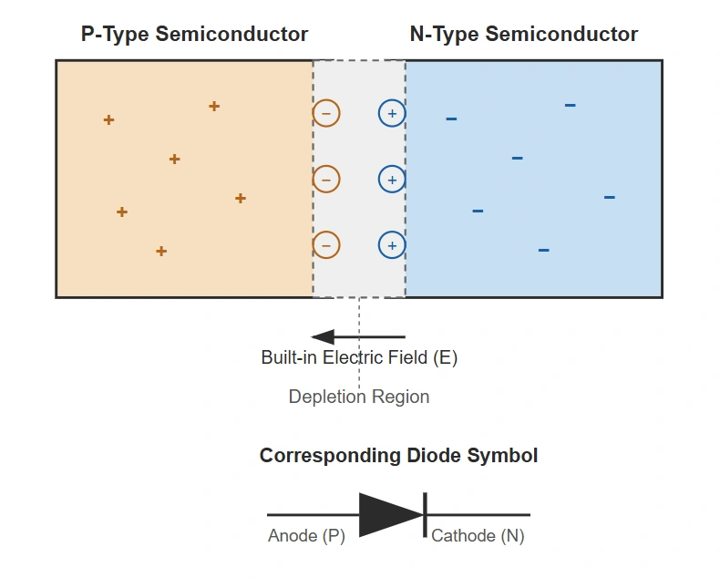
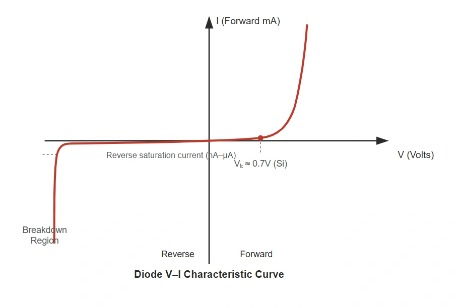
A PN junction is formed when a P-type semiconductor (doped with acceptor atoms, creating an excess of “holes”) is joined with an N-type semiconductor (doped with donor atoms, creating an excess of free electrons). At the junction, electrons and holes diffuse across the boundary and recombine, leaving behind a narrow region depleted of free charge carriers — the depletion region. This region creates a built-in electric field and a built-in potential barrier (approximately 0.7 V for silicon, 0.3 V for germanium) that opposes further diffusion.
Applying an external voltage changes the width of this depletion region:
- Forward bias (P-side positive relative to N-side): the depletion region narrows, the barrier lowers, and current flows easily once the bias exceeds the barrier potential.
- Reverse bias (N-side positive relative to P-side): the depletion region widens, the barrier increases, and only a very small leakage (saturation) current flows — until the reverse voltage becomes large enough to trigger breakdown.
Diode V–I Characteristics
A diode’s current-voltage (V–I) curve has three distinct regions:
| Region | Behavior |
|---|---|
| Forward bias | Current stays near zero until the “knee” voltage (≈0.7 V silicon, ≈0.3 V germanium, ≈2–3 V for typical LEDs), then rises sharply |
| Reverse bias | Only a tiny reverse saturation current flows (typically nA to µA range) |
| Reverse breakdown | Beyond the diode’s rated reverse voltage, current increases sharply (avalanche or Zener breakdown) |
Two related resistance concepts describe diode behavior at a given operating point: static (DC) resistance is simply the ratio of DC voltage to DC current at that point, while dynamic (AC) resistance is the slope of the V–I curve at that point (ΔV/ΔI) and describes how the diode responds to small signal changes — this is the value used when analyzing a diode inside a small-signal amplifier or rectifier ripple calculation.
Zener Diodes and Breakdown Mechanisms
Ordinary diodes are damaged by sustained reverse breakdown; Zener diodes are specifically designed to operate safely in reverse breakdown and hold a nearly constant voltage across a range of currents, which makes them useful as simple voltage references and shunt voltage regulators. Two physical mechanisms cause reverse breakdown:
- Zener breakdown: dominant in heavily doped junctions with breakdown voltages below about 5 V; a strong electric field directly pulls valence electrons free.
- Avalanche breakdown: dominant above about 5–6 V; accelerated carriers collide with the lattice and knock loose additional carriers in a multiplying chain reaction.
Diodes rated in the 5–6 V range typically exhibit a mix of both mechanisms, which is also why diodes in that range tend to have the best (lowest) temperature coefficient.
How Diodes Look and Behave on a Real PCB
On an assembled PCB, small-signal and rectifier diodes are almost always surface-mount (SOD-123, SMA, SMB, SMC packages) rather than through-hole, and polarity is marked with a printed band on the package that must align with a silkscreen cathode marker (a bar, a “K,” or a chamfered pad outline) on the board. Reversing a diode’s orientation during assembly is one of the most common first-article defects found during automated optical inspection (AOI) — it is also one of the easiest defects to catch early with a clear, unambiguous silkscreen design and polarity keying in the footprint.
3. Rectifiers and Filters: Turning AC into DC
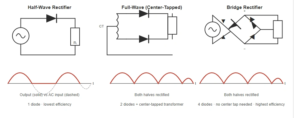
A rectifier uses one or more diodes to convert alternating current (AC) into pulsating direct current (DC). A filter then smooths that pulsating output into a steadier DC voltage suitable for powering electronic circuits.
Half-Wave, Full-Wave & Bridge Rectifiers
| Type | Diodes Required | Ripple Frequency | Typical Efficiency |
|---|---|---|---|
| Half-wave | 1 | Equal to input frequency | Lowest (only one half-cycle is used) |
| Full-wave, center-tapped | 2 (plus a center-tapped transformer) | Twice the input frequency | Higher than half-wave |
| Full-wave bridge | 4 | Twice the input frequency | Highest; no center-tapped transformer needed |
The bridge rectifier is the most widely used configuration in practical power supplies because it delivers full-wave rectification without requiring a center-tapped transformer, at the cost of a slightly higher forward voltage drop (two diode drops instead of one).
Filter Circuits: Capacitor, Inductor & LC Filters
Raw rectifier output is a pulsating DC waveform, not a flat DC level. Filters reduce this ripple:
- Capacitor (shunt) filter: a capacitor across the output charges near the peak of each pulse and discharges slowly through the load, smoothing the ripple. Larger capacitance and lighter load current both reduce ripple.
- Inductor (series) filter: an inductor opposes rapid changes in current, smoothing the waveform from the current side rather than the voltage side; more effective at higher, steadier load currents.
- LC and multiple-section filters: combine inductors and capacitors (L-section, π-section) for better ripple rejection than either element alone, at the cost of size, weight, and component count.
Clippers and Clampers
Clipper and clamper circuits use diodes for waveform shaping rather than power conversion. A clipper removes (clips) part of a waveform above or below a set reference level — commonly used for waveform shaping and input protection. A clamper shifts an entire waveform up or down without changing its shape, fixing either the positive or negative peak to a reference level — commonly used in signal-restoration and level-shifting applications.
4. Bipolar Junction Transistors (BJT): Construction, Configurations & Biasing
A BJT is a three-terminal device (Emitter, Base, Collector) built from two PN junctions in either an NPN or PNP arrangement. A small current into the base controls a much larger current flowing between the collector and emitter, which is what makes the BJT useful both as a signal amplifier and as an electronic switch.
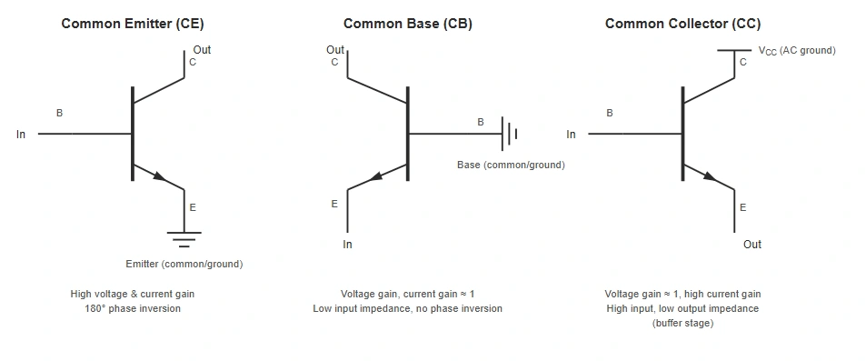
CE, CB & CC Configurations Compared
| Configuration | Voltage Gain | Current Gain | Input Impedance | Typical Use |
|---|---|---|---|---|
| Common Emitter (CE) | High | High | Moderate | General-purpose voltage amplification |
| Common Base (CB) | High | ≈1 (slightly less) | Low | High-frequency and impedance-matching stages |
| Common Collector (CC / Emitter Follower) | ≈1 | High | High | Buffering / impedance matching between stages |
Why Biasing Matters: Operating Point & Stability
Before a BJT can amplify a signal cleanly, it must be biased into its active region with a stable DC operating point (also called the Q-point) — a fixed combination of base current, collector current, and collector-emitter voltage around which the AC signal swings. Without correct biasing, the output signal clips or distorts. Common biasing schemes, in increasing order of stability against temperature drift and transistor-to-transistor variation, are:
- Fixed bias: simplest circuit, but poor stability — the operating point drifts significantly with temperature and with beta (current gain) variation between transistors.
- Collector-to-base bias: adds negative feedback from the collector to the base, improving stability over fixed bias.
- Voltage-divider (self) bias: the most widely used scheme in practical designs; a resistor divider sets a stable base voltage largely independent of beta, giving the best stability of the three.
BJT as a Switch vs BJT as an Amplifier
The same transistor can be operated in two very different modes depending on how it is biased. Driven fully into saturation (base current large enough that collector current is limited only by external resistance) or fully into cutoff (no base current, no collector current), the BJT behaves like an on/off switch. Biased instead into the active region, between saturation and cutoff, it behaves as a linear amplifier where collector current tracks base current proportionally.
BJT Packages and PCB Footprint Considerations
Common discrete BJT packages include through-hole TO-92 (still widely used for prototyping and low-volume production) and surface-mount SOT-23 (the standard choice for automated assembly). Footprint accuracy matters more than it might appear: an undersized thermal pad or insufficient copper area on a power transistor’s collector pad can cause thermal derating in real operation even when the schematic and datasheet values look correct on paper — this is one of the gaps between theoretical circuit analysis and a physical, manufactured board.
5. Field-Effect Transistors (FET, JFET & MOSFET)
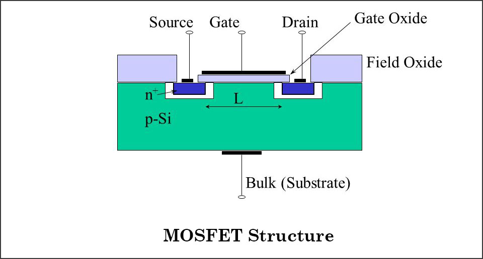
Unlike a BJT, which is a current-controlled device, a field-effect transistor is a voltage-controlled device: a voltage applied at the gate terminal controls current flow between the source and drain, with (ideally) no gate current at all.
JFET Construction & Pinch-Off Voltage
A Junction FET consists of a channel of one semiconductor type (N-channel or P-channel) with a gate region of the opposite type diffused into it, forming a PN junction along the channel. As reverse-bias gate-to-source voltage increases, the depletion region around the gate junction widens and narrows the conducting channel. At the pinch-off voltage, the channel is fully constricted and drain current levels off (saturates) rather than continuing to rise with drain-source voltage.
MOSFET: Enhancement vs Depletion Mode
A MOSFET (Metal-Oxide-Semiconductor FET) uses an insulated gate (typically silicon dioxide) rather than a PN junction, giving it an extremely high input impedance.
- Enhancement-mode MOSFET: normally off with zero gate-source voltage; a conducting channel must be “enhanced” into existence by applying a gate voltage beyond the threshold voltage. This is by far the more common type in digital logic and power-switching applications.
- Depletion-mode MOSFET: normally on with zero gate-source voltage; a channel already exists and must be “depleted” (reduced) by an applied gate voltage to reduce or stop current flow.
BJT vs FET: Which One and When
| Factor | BJT | FET / MOSFET |
|---|---|---|
| Control type | Current-controlled | Voltage-controlled |
| Input impedance | Moderate | Very high |
| Switching speed | Generally slower | Generally faster (especially MOSFETs) |
| Noise performance | Good | Generally better at high frequency |
| Common role in modern PCBs | Small-signal amplification, simple switching | Power switching, digital logic, high-impedance sensor interfaces |
6. From Components to Circuits: Amplifiers, Feedback & Oscillators
What Makes a Circuit an “Amplifier”?
An amplifier circuit uses a biased BJT or FET, together with resistors and coupling/bypass capacitors, to increase the amplitude of a small input signal while preserving its shape. The transistor itself only provides gain; the surrounding passive network sets the operating point, defines the frequency response, and couples the signal in and out without disturbing the DC bias. Engineers commonly use small-signal models (h-parameters for BJTs, or simplified transconductance models for FETs) to predict gain, input impedance, and output impedance before ever building the circuit.
For a full walkthrough of BJT and FET small-signal analysis, h-parameters, and practical biasing design techniques, see our companion guide, Transistor Biasing and Amplifier Design: BJT & FET Explained.
Why Feedback and Oscillators Matter in Real Circuits
Feeding a portion of a circuit’s output back to its input — feedback — changes how the circuit behaves. Negative feedback trades away some raw gain in exchange for better stability, lower distortion, wider bandwidth, and more predictable performance, which is why it is used in the vast majority of practical amplifier and regulator designs. Positive feedback, when the loop gain and phase conditions defined by the Barkhausen criterion are satisfied, causes a circuit to oscillate on its own — generating a continuous waveform without an external AC input. This is the basis of oscillator circuits used to generate clock signals, carrier frequencies, and timing references throughout electronics.
For oscillator types, design examples, and the difference between RC, LC, and crystal oscillators, see our companion guide, Feedback Amplifiers and Oscillator Circuits: A Practical Guide.
7. Special-Purpose Semiconductor Devices
Beyond standard diodes, BJTs, and FETs, a handful of specialized semiconductor devices show up regularly in both coursework and real designs:
- Silicon-Controlled Rectifier (SCR): a four-layer device that, once triggered, continues conducting until current drops below a holding value — used in AC power control and switching.
- Tunnel diode: exploits quantum tunneling to produce a region of negative differential resistance, useful in very high-frequency oscillators and switching circuits.
- Varactor (varicap) diode: its junction capacitance changes with applied reverse voltage, making it useful as a voltage-controlled capacitor in tuning and frequency-modulation circuits.
- Photodiode: generates or modulates current in response to incident light, forming the basis of optical sensors and receivers.
- Unijunction Transistor (UJT): a simple three-terminal device commonly used to build relaxation oscillators and timing circuits.
8. Passive vs Active Components at a Glance
Everything discussed above — diodes, BJTs, and FETs — falls into the broader category of active components: devices that can control, switch, or amplify a signal and generally require an external power source to do so. Passive components — resistors, capacitors, and inductors — cannot amplify a signal and typically only store, dissipate, or filter energy already present in the circuit, but they are just as essential, since they set bias points, filter frequencies, and shape timing in every circuit discussed in this guide.
For a deeper breakdown of both categories with real-world examples and PCB-level considerations, see our guides on Active vs Passive Electronic Components and The 10 Most Commonly Used Electronic Components.
9. From Circuit Theory to a Real PCB: Design Workflow
Schematic → Layout → Prototype → Assembly
Turning the devices and circuits covered in this guide into a working product generally follows four stages: capturing the circuit as a schematic in EDA software, translating that schematic into a physical PCB layout (component placement and copper routing), fabricating and testing a small-batch prototype, and finally moving to full assembly once the design is verified. Our guides on PCB Design: From Concept to Final Artwork and A Comprehensive Guide to PCB Assembly walk through each of these stages in detail.
Common Mistakes When Moving from Theory to Board
Circuit theory assumes ideal components and infinite bandwidth; a real PCB does not. A few of the most common gaps between a correct schematic and a working board include:
- Ignoring parasitic elements: every trace has parasitic inductance, and every pad has parasitic capacitance. In high-frequency amplifier and oscillator circuits, these parasitics can shift the actual operating frequency or introduce unwanted feedback paths that were never in the original schematic.
- Undersized thermal relief on power devices: a BJT or MOSFET biased correctly on paper can still overheat and drift out of its intended operating point if its footprint doesn’t provide enough copper area or thermal vias to dissipate heat.
- Poor grounding and return-path planning: amplifier stages are especially sensitive to ground bounce and shared return paths, which can introduce noise or unintended feedback that behaves like the negative-feedback and oscillator effects discussed in Section 6 — except unintentional and uncontrolled.
Running a Design for Manufacturing (DFM) check before ordering a prototype catches many of these issues — footprint mismatches, insufficient clearances, and missing thermal relief — before they turn into a failed board.
Frequently Asked Questions
What is the difference between an electronic device and an electronic circuit?
An electronic device (such as a diode or transistor) is a single component that controls, switches, or amplifies current. An electronic circuit is an interconnected network of such devices, along with passive components, arranged to perform a specific function, such as rectification or amplification.
What are the main topics covered in an Electronic Devices and Circuits (EDC) course?
Most EDC curricula cover, in order: PN junction diodes and their V–I characteristics; rectifiers and filters; bipolar junction transistors (construction, configurations, and biasing); field-effect transistors (JFET and MOSFET); small-signal amplifier analysis; and feedback amplifiers and oscillators.
What is the difference between a BJT and a FET?
A BJT is current-controlled — a small base current controls a larger collector current. A FET is voltage-controlled — a gate voltage controls current between the source and drain with essentially no gate current. FETs generally offer much higher input impedance than BJTs.
Why is transistor biasing necessary?
Biasing establishes a stable DC operating point so that an AC input signal can be amplified without clipping or distortion. Without proper biasing, the transistor may sit in cutoff or saturation for part of the signal cycle, distorting the output.
What is the difference between a rectifier and a filter?
A rectifier converts AC into pulsating DC using diodes. A filter, placed after the rectifier, smooths that pulsating DC into a steadier voltage using capacitors, inductors, or a combination of both.
10. Conclusion
Electronic devices and circuits form a continuous chain: semiconductor physics explains how a single PN junction behaves, that behavior scales up into diodes, BJTs, and FETs, those devices combine into rectifiers, amplifiers, and oscillators, and those circuits ultimately have to be laid out, fabricated, and assembled onto a physical PCB. Understanding the theory is the first half of the job; understanding how that theory holds up — or doesn’t — on a real, manufactured board is the second half, and it is where a lot of otherwise well-designed circuits run into trouble. The companion guides linked throughout this article go deeper into transistor amplifier design, oscillator circuits, and the practical PCB workflow for anyone ready to take a circuit from theory to a working prototype.
Ready to Take Your Circuit from Theory to a Manufactured PCB?
Get an instant PCB quote, run a free DFM check on your layout, or order a PCB prototype to move your design from schematic to a working board.