
 Surface


Stacy Lu

 NextPCB Capabilities
Printed Circuit Boards
NextPCB Capabilities
Printed Circuit Boards
 PCB Assembly
 Layer Buildup
 SMD-Stencils
 PCB Design-Aid & Layout
 Mechanics
 Quality
 Drills & Throughplating
 Factory & Certificate
 PCB Assembly Factory Show
Certificate
PCB Assembly Factory Show
Certificate
Support Team
Feedback:
support@nextpcb.com


Introduction
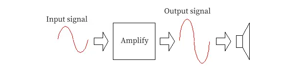
An amplifier is a device designed to increase the voltage or power of an input signal. It consists of components like vacuum tubes, transistors, power transformers, and other electrical elements. Amplifiers are widely used in various devices such as communication systems, broadcasting, radar, television, and automatic control systems.
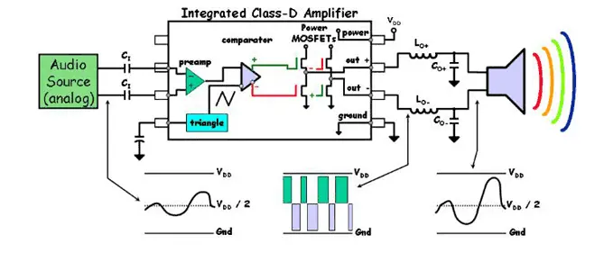
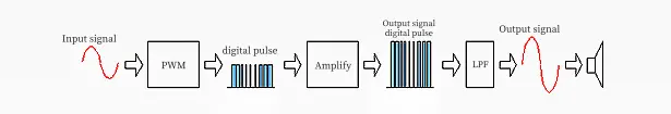
Class D Amplifier Board is an electronic circuit board designed to drive audio amplification using a Class D architecture. In a Class D amplifier, the output stage operates in a switching mode, where the transistors switch on and off rapidly, creating a pulse-width modulation (PWM) signal. This signal is then filtered to recover the audio signal, making it highly efficient compared to traditional analog amplifiers. Class D amplifiers are used in applications requiring high efficiency, low heat generation, and compact design, such as in audio systems, home theater systems, and portable speakers. The Class D Amplifier Board typically includes components such as MOSFETs, capacitors, inductors, and resistors, which are organized on the PCB to optimize performance and minimize signal distortion.
In this blog, we will explore key design strategies for Class D amplifier boards, focusing on thermal management, PCB layout optimization, and cost-effective solutions and discuss the growing demands of the Indian market.
Table of Contents
In the context of the growing prevalence of high-performance and compact electronic devices, amplifier circuit board design must focus primarily on system efficiency. For Indian engineers and designers seeking global competitiveness, selecting the right architecture is the crucial first step toward achieving reliability and reducing Total Cost of Ownership (TCO).
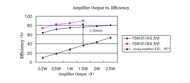
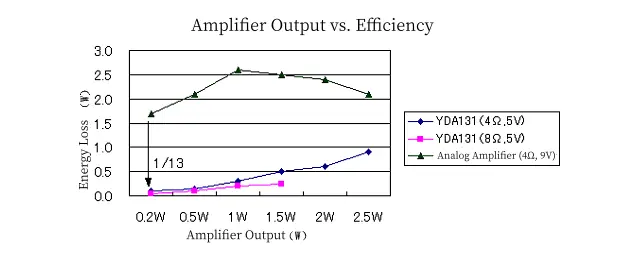
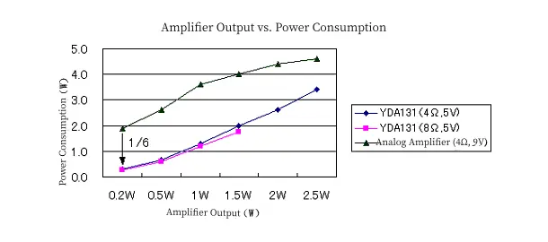
Power consumption is the foremost factor affecting the performance, longevity, and thermal management cost of electronic devices. While traditional linear amplifiers (e.g., Class AB) typically achieve efficiencies of only 50% to 70%, Class D amplifiers, utilizing switching mode operation, can reach higher efficiencies of 85% to 90%. This inherent high efficiency directly translates into less electrical energy dissipated as heat.
The Class D architecture is the ideal choice for high-efficiency design, especially in regions with higher ambient temperatures like India, as it effectively reduces power consumption and improves the thermal design margin. If power dissipation Pdiss can be significantly reduced by 30% to 40%, the thermal solution can be effectively simplified. Minimizing heat generation not only prolongs component lifespan but also reduces costs, sometimes even allowing designers to omit expensive heat sinks or fans. Therefore, adopting the Class D architecture is not merely an electrical decision but a fundamental Value Engineering (VE) step, as it directly impacts both the Bill of Materials (BOM) cost and Category II and III elements of the manufacturer-defined Printed Circuit Board (PCB) fabrication cost.
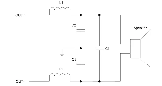
Class D amplifiers deliver the audio signal by utilizing a Pulse Width Modulation (PWM) output waveform. Many modern Class D amplifiers leverage advanced modulation techniques that, in various applications, can eliminate the need for an external low-pass filter, thereby saving board space and reducing system cost. While this "filterless" design offers cost and space advantages, it requires the speaker load to remain inductive at the amplifier's switching frequency. This ensures maximum output power capability and prevents excessive high-frequency switching energy from dissipating in the speaker resistance.
However, designers must be aware of the unique challenges posed by the Class D architecture. For instance, while a full-bridge Class D amplifier typically maintains a unidirectional energy flow from the supply to the load, a half-bridge design can exhibit bidirectional energy flow, leading to "Bus pumping" phenomena—where the bus capacitors are charged in reverse by energy flowing from the load back to the supply—mainly occurring at low audio frequencies (typically below 100Hz). Furthermore, eliminating the external filter, while cost-saving, means high-frequency PWM switching energy travels along the output traces to the speaker, significantly increasing the risk of Electromagnetic Interference (EMI) radiation from the output traces. The cost saved on the filter must therefore be reinvested in superior, more stringent EMI/EMC control measures in the PCB layout, such as optimized grounding and stack-up structures.
Total Harmonic Distortion (THD or THDi) is a key metric measuring the harmonic distortion present in a signal, defined as the ratio of the sum of the powers of all harmonic components to the power of the fundamental frequency. In audio systems, lower THD indicates that the equipment produces a more accurate reproduction of the audio, while in radio communications, it results in less unintentional interference.
THD is measured by applying a spectrally pure sine wave to the amplifier in a defined circuit configuration and observing the output spectrum. Designers must recognize that the quality of THD performance depends not only on the amplifier chip's inherent linearity but is also highly sensitive to various parameters: the PCB layout, grounding, power supply decoupling, the applied load, and the supply voltage. For Class D amplifiers, the THD performance is often a direct reflection of the PCB layout quality. If the layout introduces Power Integrity (PI) issues or EMI-coupled noise, this noise modulates the input signal, creating harmonics.
Therefore, the key to achieving ultra-low THD (typically below 0.1%) lies in whether the PCB layout effectively shields the sensitive analog stage from high-frequency switching noise interference. THD test failures can frequently be traced back to layout defects rather than inherent component flaws.
| Metric | Class AB (Linear) | Class D (PWM) | Design Implication (Indian Market Focus) | Reference |
|---|---|---|---|---|
| Efficiency (Typical) | 50% - 70% | 85% - 90% | Core: High efficiency minimizes power dissipation, reducing the need for large heat sinks and lowering BOM cost. | 1 |
| Thermal Management | High Heat Generation | Low Heat Generation | Constraint: Requires large, costly thermal solutions; high risk in high ambient temperatures like 50°C environment. | 4 |
| Layout Complexity | Moderate (Analog) | High (Mixed-Signal/Digital) | Focus: Requires mastery of high-frequency switching handling, grounding, and EMI suppression techniques. | 3 |
| THD Sensitivity | High (Relies on component linearity) | High (Highly sensitive to PI/EMI noise coupling) | Validation: Requires clean power rails and strict isolation to achieve target audio purity. | 9 |
When designing high-power amplifier circuit boards, particularly for applications that may face high ambient temperatures (such as in India), thermal management must be treated as a core part of the design process. Reliability mandates that the designer views the PCB itself as a critical thermal element, not just a conductor of electricity.
Effective thermal management extends component lifespan. Designers should set stringent targets, such as keeping the temperature of critical components below 85°C even under full load. Given that ambient temperatures in the Indian market can approach 50°C, this presents a severe thermal design challenge. While many semiconductor components are tested in the military temperature range (-55°C to 125°C), continuous operation near the maximum limit significantly shortens their useful life.
When the ambient temperature reaches 50°C, the temperature rise margin (ΔT = Tjunction - Tambient) between the chip junction temperature (Tjunction) and the ambient temperature (Tambient) becomes very small. If the goal is to maintain the junction temperature below 85°C, the maximum allowable temperature rise is only 35°C. This stringent margin demands that the design must first choose a high-efficiency Class D chip to minimize heat generation, and subsequently actively manage heat by utilizing large copper pours and optimized Thermal Vias to reduce the junction-to-ambient thermal resistance (θJA).
The PCB layout is the primary vehicle for implementing passive cooling. For surface-mounted power components (such as SMD transistors or power ICs), Thermal Vias are indispensable.
Thermal Vias should be placed directly under or near heat-generating components. For example, for a power IC dissipating 5W, an array of 10-15 vias with a diameter of 0.3mm is recommended. This high-density thermal via array significantly reduces thermal resistance, helping to lower component temperatures by 10°C to 20°C. To enhance cooling effectiveness, these thermal vias must be connected to a large copper plane or a dedicated ground plane to effectively spread the heat over a wider area.
Design optimization should aim to minimize heat generation before it becomes a thermal management issue. This includes selecting MOSFETs with low on-resistance (Rds(on)) or BJTs with low saturation voltage to reduce power loss. Simultaneously, ensuring the amplifier output is correctly matched to the speaker impedance also helps minimize wasted power dissipation.
> Recommend reading: What's the difference between MOSFET and BJT and how to choose?
| Parameter | Recommendation | Rationale | Reference |
|---|---|---|---|
| Placement | Directly under or near high-heat components (Power ICs, MOSFETs). | Maximizes the direct conduction path for heat from the chip junction to the copper plane. | 1 |
| Density (Example) | Array of 10-15 vias for components dissipating ≈ 5W. | Achieves significant temperature reduction (10-20°C), crucial in 50°C environments. | 1 |
| Via Diameter | Typically 0.3mm (12 mil) drill, plated with copper. | Balances thermal performance, manufacturing cost, and board space utilization. | 1 |
| Connection | Connect vias to a large dedicated ground plane or internal copper planes. | Ensures heat is spread over the maximum surface area for convection/conduction. | 12 |
Standard FR-4 material offers only modest thermal conductivity (0.3-0.5 W/mK), which may be insufficient for extremely high-power applications requiring thermal integrity. In industrial, defense, or extreme high-power systems (such as large professional audio or ruggedized defense electronics) in India, the use of high-performance substrate materials must be considered.
Ceramic substrates (e.g., aluminum oxide) can achieve thermal conductivities of 20-30 W/mK, while aluminum nitride can reach 170-250 W/mK. Although these advanced materials significantly increase initial fabrication costs, their superior thermal performance allows for operation at higher power densities and dramatically improves Mean Time Between Failures (MTBF). For mission-critical applications where failure costs are extremely high (e.g., telecom infrastructure or defense equipment), Value Engineering analysis favors selecting high-performance materials to maximize product lifespan, justifying the high initial material expense over the product's life cycle.
A Class D amplifier circuit board is inherently a mixed-signal challenge, requiring strict isolation and robust electromagnetic control to ensure audio quality and system reliability.
To achieve compact design and excellent high-frequency performance, Surface Mount Technology (SMT) is essential for modern amplifier circuit boards. SMT minimizes parasitic capacitance and inductance, leading to cleaner sound and less noise.
In routing practice, high-frequency traces (PWM switching lines) must be kept short and direct. Heat-generating components should be placed near heat sinks or areas with good airflow, fully utilizing thermal vias for heat conduction. In high-frequency buses or digital control lines, differential pair routing must protect signal integrity. Designers should avoid using vias in differential traces; if unavoidable, the same number of vias must be used on both traces, and an anti-pad shared by two vias must be employed to minimize parasitic capacitance.
Power Integrity is the key factor in ensuring Class D amplifier stability and low distortion. Power planes, power vias, and return paths must possess extremely low impedance to minimize power noise and signal distortion. High resistance leads to power loss as heat and causes signal integrity issues, potentially resulting in component failure.
An effective power decoupling strategy is crucial for stabilizing bus voltage, especially to counteract the "Bus pumping" effect that can occur in half-bridge Class D stages. Low-impedance planes and superior decoupling design must be prioritized in a successful Class D PCB design, on par with signal routing. If there are flaws in power integrity (i.e., the quality of power delivery), such as voltage dips or ripple on the power rails, this noise will directly couple into the output stage, causing a sharp deterioration in the amplifier's performance (THD). A failure in power integrity immediately manifests as a degradation in audio quality (THD).
The high-frequency switching characteristic of Class D amplifiers makes them susceptible to EMI issues. For effective shielding, especially when dealing with high-frequency switching noise, it is recommended to use an alternating layer stack-up structure: Signal Layer → Ground/Power Layer → Signal Layer. To ensure symmetric return paths, the total number of layers should preferably be even (e.g., 4, 6, or 8 layers).
Isolation is Key. Strict separation of AC and DC/analog circuits is mandatory, employing electrical isolation and shielding components to manage interference between different systems. Never route traces across isolation barriers. For grounding strategy, utilize dedicated ground planes and ground vias. The ground plane not only provides a low-impedance return path for signals but is also a critical medium for effective heat dissipation.
In a market aspiring to be a global manufacturing hub, like India, adherence to IPC and high-reliability standards is the foundation for establishing product trust and quality. For professional engineers, these standards provide a passport into the international supply chain.
IPC standards are widely applied across the global electronics industry to clarify industry expectations and ensure quality, reliability, and consistency.
IPC-2221 (Design Foundation): This is the generic standard for PCB designers, covering design elements such as layout, conductor spacing, and materials that impact both performance and manufacturability. Following this standard during the design phase significantly reduces errors and production challenges.
IPC-6012 (Performance Assurance): This standard focuses on the qualification, performance, and durability of Rigid PCBs, specifying requirements for electrical, thermal, and mechanical properties. Boards meeting this standard reliably withstand expected wear and stress, ensuring a longer product lifespan.
The Indian automotive electronics market, particularly Electric Vehicles and Advanced Driver-Assistance Systems (ADAS), is growing rapidly, placing higher reliability demands on components.
The AEC-Q100 standard defines qualification requirements for semiconductor components in the automotive environment, often mandating operation at extreme temperatures up to 150°C. For Tier 1 suppliers, using AEC-Q100 qualified Class D audio amplifier ICs (e.g., chips from STMicroelectronics or Texas Instruments) is mandatory. This further requires high-temperature testing during the assembly and packaging stages, such as 100% hot testing at 125°C. Designers must understand that satisfying AEC-Q100 is the entry-level requirement for the automotive supply chain, imposing strict constraints on component selection, thermal design margins, and validation processes.
Indian designers rely on global authorized distributors to procure specialized audio ICs, including those from Cirrus Logic, Infineon, TI, and STMicroelectronics. Choosing manufacturers that offer high-quality reference designs and application notes is crucial for managing complex Class D modulation techniques, minimizing design risks and time-to-market.
In a highly competitive market, engineering success means delivering reliable functionality at the most competitive cost. Value Engineering (VE) is a systematic process designed to increase a product's value by improving its function while reducing the overall costs.
VE for an amplifier circuit board involves systematically reviewing the Bill of Materials (BOM), optimizing production processes, and improving the supplier base. This analysis must be proactively conducted in the early design stages to prevent late-stage cost overruns from eroding expected profits.
Key focus areas for VE include:
The cost of a rigid PCB is driven by complexity requirements, particularly those in Categories II and III. Complexity primarily relates to materials (FR4 versus CEM-1), layer count (1 to 36 layers available), and size.
While single or double-layer boards are the cheapest to fabricate (with base board prices as low as ₹60 to ₹350 per piece), the technical demands of a Class D amplifier often necessitate a 4- or 6-layer stack-up structure to effectively manage EMI and PI.
> Recommend reading: Custom PCB and PCBA Cost Analysis: How to Optimize Design and Reduce Expenses
Designers must perform a trade-off analysis. While restricting the design to a 2-layer board can reduce Category III manufacturing costs, a high-power Class D amplifier on a 2-layer board will almost certainly fail EMI compliance or suffer degraded THD performance due to the lack of stable ground planes and return paths. This leads to costly design reiterations or regulatory re-certification (i.e., approval risk).
Therefore, Value Engineering analysis may conclude that increasing the layer count (e.g., upgrading to 4 layers) is actually a cost-saving measure. By ensuring first-pass success for EMI compliance and achieving superior reliability, one avoids the exponentially greater subsequent costs associated with field failures, rework, or design respin.
The Indian government is actively promoting the localization of advanced electronic components, including copper-clad laminates (CCL) and substrates. Leveraging Indian Supportive PCB services (such as quick turnarounds offered by NextPCB) can shorten supply lead times and improve sourcing resilience, better mitigating global supply chain fluctuations. While high-end ICs currently rely on imports, optimizing the global procurement of PCBs and mechanical parts maximizes supply chain risk reduction. Designers should actively collaborate with IPC-compliant local manufacturers to maximize localization benefits.
The future trend for amplifier circuit boards involves the deep integration of digital controls and advanced algorithms, which introduces new challenges for mixed-signal layout.
Modern market competition is driven by Digital Signal Processing (DSP)-enabled software features, such as customizable equalization, spatial audio rendering (e.g., Dolby Atmos), and adaptive noise cancellation. DSP chips must balance processing power with efficiency.
Design Requirement: The PCB layout must accommodate the DSP's high-speed interfaces (e.g., memory and complex buses). The value of DSP integration lies in its ability to adjust audio in real-time through complex mathematical models, enhancing clarity and optimizing power consumption.
The integration of DSP introduces new Signal Integrity challenges. High-performance DSPs typically require high-speed communication buses (e.g., DDR). High-speed signals demand strictly controlled impedance and clean return paths. Consequently, the integration of DSP accelerates the need for multi-layer PCB stack-ups (6 layers or more) to meet the High-Speed Digital (HSD) Signal Integrity (SI) requirements. This complexity can even surpass that of the Class D power stage itself, with the SI demands of the digital "brain" starting to dominate the overall board complexity.

Smart amplifier circuit boards increasingly integrate wireless modules (such as ESP32 or STM32 development boards) to enable remote control and integration into smart home ecosystems.
Layout Challenges: The coexistence of Radio Frequency (RF) components and high-power audio stages is a classic mixed-signal problem. Designers must strictly isolate the digital control/RF section from the high-current power amplification stage to prevent noise coupling, thereby maintaining audio quality and regulatory compliance.
The automotive sector, driven by the adoption of Electric Vehicles (EVs) and the demand for high-fidelity audio, is a key driver for PCB market growth.
Automotive amplifier circuit boards have extremely high technical requirements, including high vibration resistance, extreme temperature range compliance (AEC-Q100), and an increasing adoption of advanced technologies like flexible PCBs (the fastest-growing segment) and Substrate-Like PCBs (SLP) for miniaturization. In the future, Artificial Intelligence (AI)-driven tools will be used to automate complex automotive PCB layouts and simulations, improving design efficiency and manufacturing precision.
Designing high-reliability amplifier circuit boards is a multi-disciplinary system engineering challenge, where success hinges on the comprehensive management of electrical, thermal, electromagnetic, and cost factors. For Indian engineers, combining global best practices with the local manufacturing environment is key to gaining a competitive advantage.
Architecture Optimization as the Primary Cost Control Tool: The design must be based on the Class D architecture, leveraging its high efficiency to fundamentally reduce heat generation— which is more cost-effective than compensating later with expensive thermal hardware.
Thermal Design Must Be Conservative and Proactive: Given the high ambient temperatures in India, designers must adopt aggressive passive cooling strategies, including high-density thermal via arrays and utilizing large copper planes to reduce thermal resistance. The goal is to maintain critical component junction temperatures below the safe threshold of 85°C. For mission-critical applications, high-performance substrate materials should be considered based on VE analysis to trade higher initial cost for extended MTBF.
Layout Dictates Quality (THD): The low THD and EMI compliance of a Class D board directly depend on the quality of Power Integrity (PI) and mixed-signal isolation. Engineers must employ optimized multi-layer stack-up structures (4 layers or more recommended), ensuring low-impedance return paths and power decoupling to effectively suppress high-frequency switching noise.
Adherence to Standards Guarantees Supply Chain Success: Strict compliance with design and performance standards like IPC-2221 and IPC-6012 is fundamental to ensuring product trustworthiness globally and fostering local supply chain stability. For emerging automotive applications, AEC-Q100 qualification is the mandatory quality gate.
Strategic Value Engineering: VE should be conducted early in the design process to balance the manufacturing cost introduced by complexity against the potential savings from reliability. In EMI/PI challenging Class D designs, increasing the layer count to ensure first-pass design success is often more economical than insisting on the minimum layer count. Simultaneously, actively utilizing the growing trend of local PCB fabrication and component sourcing maximizes supply chain resilience.

Still, need help? Contact Us: support@nextpcb.com
Need a PCB or PCBA quote? Quote now

