PCB Assembly
Arya Li, Project Manager at NextPCB.com

 NextPCB Capabilities
Printed Circuit Boards
 Process Capabilities
 PCB Design-Aid & Layout
 Quality
 Drills & Throughplating
 Factory & Certificate
 PCB Assembly Factory Show
Certificate

Support Team
Feedback:
support@nextpcb.com


A 77 GHz automotive radar board is small, but it is one of the least forgiving PCBs you can order. The antenna is etched into the copper, the signal path is only a few millimetres long, and small errors in dielectric thickness, copper roughness or etch width show up directly as lost range or a shifted frequency. This guide covers the stack-up, the copper, the antenna etch and the files to send your PCB manufacturer. For the wider ADAS picture, read our ADAS PCB design guide. For NextPCB's automotive range, see our automotive radar PCB and PCBA solutions.
At 77 GHz the free-space wavelength is about 3.9 mm (299.8 mm/ns divided by 77 GHz). Inside a laminate with a dielectric constant near 3.0, the wavelength is shorter again, roughly 2.2 to 2.5 mm depending on the line geometry. This is an estimate for orientation only. Your simulation sets the real value.
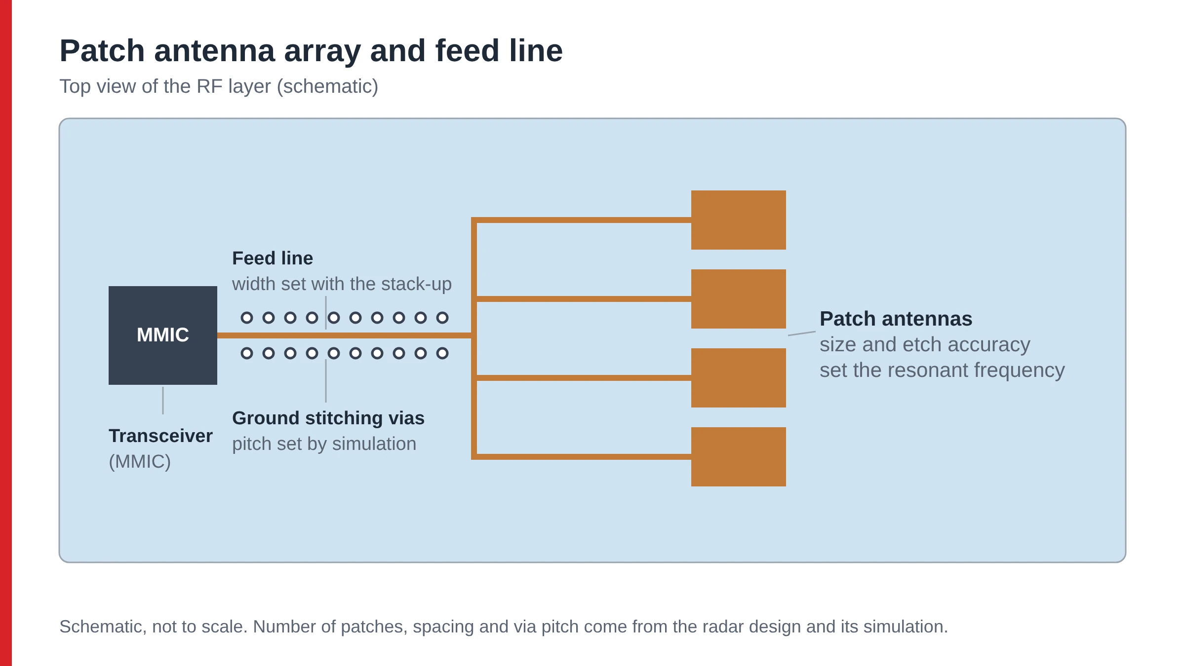
A patch antenna is about half a guided wavelength long, so its dimensions are around a millimetre. A few tens of microns of over-etch is a visible fraction of that. That is why radar boards are specified on dielectric thickness, copper profile and etch accuracy, not only on layer count.
High-frequency laminate costs more than FR-4, so radar boards normally use it only where the RF signal travels and use FR-4 for everything else.
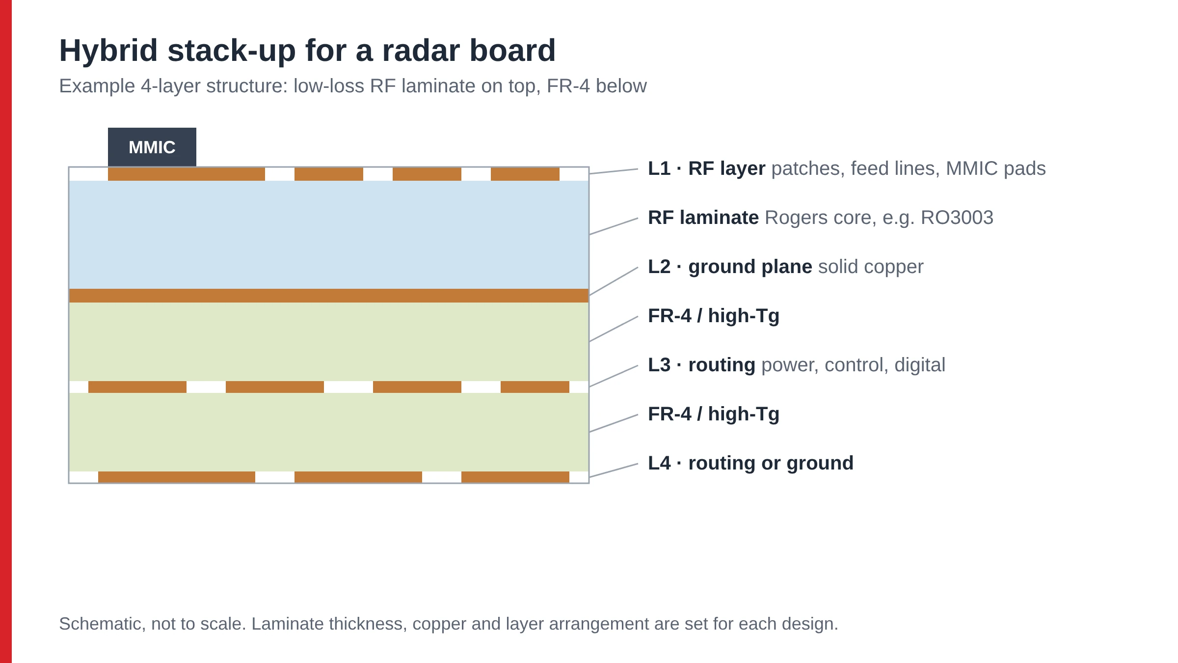
NextPCB currently supports a single Rogers core laminated with FR-4 for 2 to 6 layer boards, and pure stack-ups built from the same Rogers model. Our Rogers PCB capabilities page shows the 4-layer and 6-layer structures. If your design needs more than one Rogers core in the same board, send it for engineering review before you commit to the stack-up.
On our materials table, RO3003 is the laminate listed up to 77 GHz. The other Rogers materials we list for general high-frequency work, RO4003C and RO4350B, are listed up to 30 GHz.
| Material | Max frequency | Dk at 10 GHz | Df at 10 GHz | Type |
|---|---|---|---|---|
| RO3003 | 77 GHz | 3.00 | 0.0013 | PTFE with ceramic filler |
| RO4003C | 30 GHz | 3.38 | 0.0027 | Hydrocarbon, ceramic, woven glass |
| RO4350B | 30 GHz | 3.48 | 0.0037 | Hydrocarbon, ceramic, woven glass |
Note the test frequency. Datasheet Dk and Df values are quoted at 10 GHz. They show how materials rank against each other, but they are not the loss you will see at 77 GHz. At 77 GHz, loss also depends on the copper profile, the line width and the dielectric thickness. When you compare laminates, ask which test method and frequency each number came from.
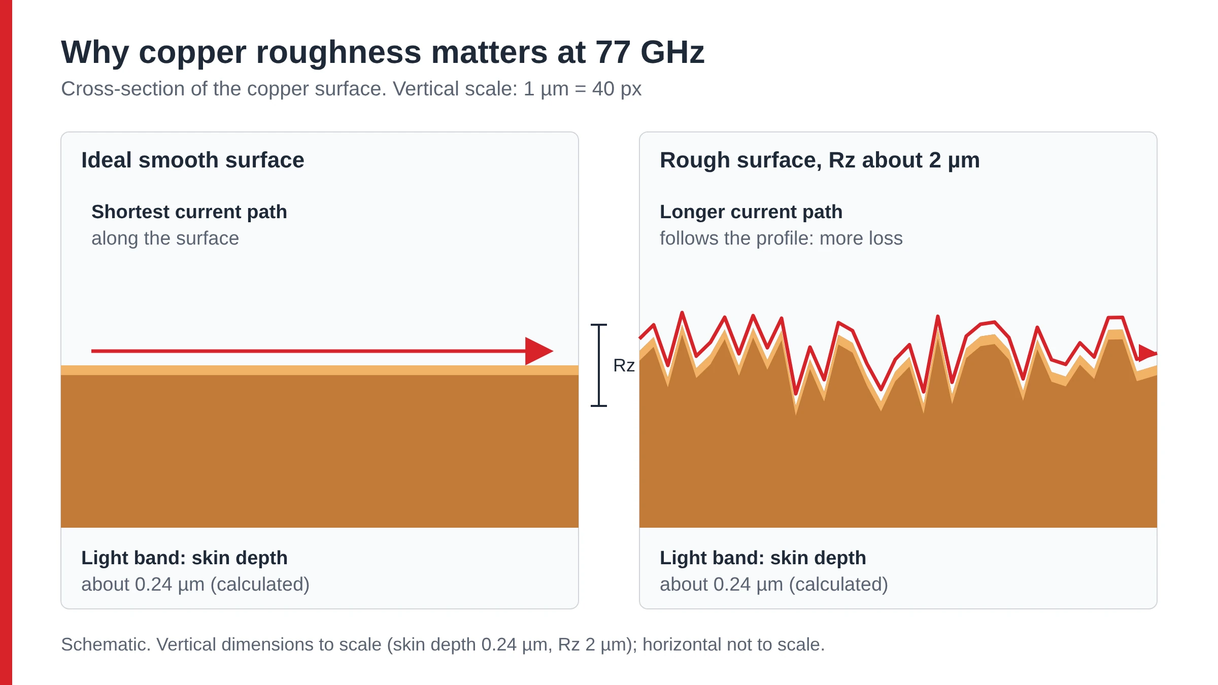
At high frequency, current flows in a thin layer at the surface of the copper. For copper at 77 GHz that skin depth is about 0.24 µm (calculated from the standard formula). Rough copper forces the current to follow the surface profile, so the path is longer and the conductor loss is higher.
Radar design guidance commonly asks for very low profile copper with a roughness (Rz) below 2 µm on the RF layer. Electrodeposited foils come in several grades, such as HTE, RTF, ULP and HVLP, and rolled-annealed (RA) copper is smoother again. Lower-profile grades trade roughness against adhesion, so the choice is a design decision to agree with your manufacturer.
The copper on a laminate such as RO3003 is specified when the material is ordered. Do not assume a default. State the foil type and roughness you need in your fabrication notes, and we will confirm what can be supplied in engineering review.
Radar design guidance often asks for patch dimensions held to about ±10 µm, because over-etching shifts the resonant frequency. Treat this as a design requirement to discuss, not as a standard fabrication tolerance. A general line-width tolerance of ±10% on a 0.3 mm feed line is ±30 µm, which is three times wider than ±10 µm.
If your antenna depends on a tight etch, tell the manufacturer which features are critical and what you need. Compensation applied in CAM, test coupons and measurement of the critical features can then be agreed before production. Our Rogers page lists a minimum trace and space of 3.5 / 3.5 mil and a minimum hole size of 0.15 mm.
| Item | Why it matters |
|---|---|
| Stack-up drawing with laminate model and thickness | The dielectric thickness under the antenna and feed sets the impedance and the resonant frequency. |
| Copper type and roughness for the RF layer | Sets conductor loss at 77 GHz. Confirm what can be supplied. |
| Impedance targets and tolerance | Lets the stack-up and line widths be checked together. |
| Critical antenna features and etch requirement | Identifies which dimensions need compensation and measurement. |
| Surface finish | Our Rogers page lists ENIG, OSP, immersion tin and immersion silver. The finish affects loss on the RF layer, so state your choice. |
| Via and layer-transition details | Hole size, pads, anti-pads and ground via layout for the RF transitions. |
| Automotive requirements | IPC class, traceability and approval documents. See automotive PCB design and IATF 16949 certified PCB and PCBA. |
All of these are confirmed for manufacturability in engineering review before production. For related materials and high-frequency boards, see our high-frequency PCB page.
It is not recommended. FR-4 has much higher dielectric loss at millimetre-wave frequencies than low-loss laminates such as RO3003. FR-4 is normally kept for the lower layers that carry power and digital signals.
RO3003 is listed with a maximum frequency of 77 GHz. RO4003C and RO4350B are listed up to 30 GHz. See the Rogers PCB capabilities page.
We support a single Rogers core laminated with FR-4 for 2 to 6 layer boards, and pure stack-ups built from the same Rogers model. Send your stack-up for review if it needs a different structure.
No. It is a design requirement often quoted for radar antennas. Send us your critical antenna features and the tolerance you need, and our engineers will review whether it can be met.
The same principles apply: low-loss laminate on the RF layer, low-profile copper and tight control of dielectric thickness and etch. The wavelength is slightly shorter, about 3.8 mm in free space, so tolerances matter even more.
Send your stack-up and fabrication notes for an engineering review, or upload your files for a quote.

Still, need help? Contact Us: support@nextpcb.com
Need a PCB or PCBA quote? Quote now