
 Surface


Arya Li, Project Manager at NextPCB.com

 NextPCB Capabilities
Printed Circuit Boards
NextPCB Capabilities
Printed Circuit Boards
 PCB Assembly
 Layer Buildup
 SMD-Stencils
 PCB Design-Aid & Layout
 Mechanics
 Quality
 Drills & Throughplating
 Factory & Certificate
 PCB Assembly Factory Show
Certificate
PCB Assembly Factory Show
Certificate
Support Team
Feedback:
support@nextpcb.com


Table of Contents
In modern high-speed electronic system design, the Printed Circuit Board (PCB) is far more than a simple wiring substrate; it functions as a high-frequency transmission line. Characteristic Impedance (Z0) is a critical parameter of this transmission line, defined as the ratio of voltage to current along the path. Essentially, characteristic impedance is determined by the intrinsic electrical parameters of inductance (L) and capacitance (C) per unit length.
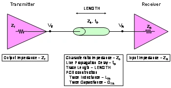
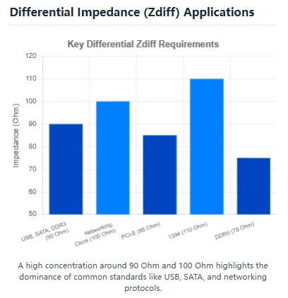
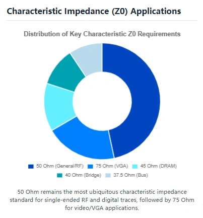
Characteristic impedance is key to ensuring Signal Integrity (SI). In high-speed digital circuits, if the PCB trace's characteristic impedance (Z0) does not precisely match the termination impedance of the driver or receiver, energy will be reflected at the connection point. These reflections travel back and forth along the transmission line, causing signal distortion, timing errors, and potential functional failure. To minimize reflections, design engineers must strictly control the PCB trace's Z0, making it match the system's specified target impedance. The industry standard target characteristic impedance (Ztarget) for single-ended signals is typically set at 50Ω. This value is a well-considered compromise, balancing signal power transfer efficiency, compatibility with standard connectors and cables, and the impedance requirements of driver and receiver chips.
> Recommend reading: PCB Trace Width Calculation: High-Current Design & Thermal Analysis
Controlled Impedance (CI) Tolerance is a hard measure of manufacturing quality. It defines the maximum allowable deviation of the measured impedance (Zmeasured) from the target impedance (Ztarget), quantified as ΔZ = Ztarget - Zmeasured. In PCB manufacturing, impedance tolerance directly reflects the precision required by the fabrication process and is classified into different levels based on application speed and complexity.
Standard CI tolerance is typically ±10%. However, as data rates continue to rise (e.g., in extremely high-speed serial buses like PCIe Gen4/5 and DDR5), timing budgets and noise margins are severely compressed, demanding more precise impedance control. Consequently, these cutting-edge applications often require high-precision tolerance, usually ±5%.
Tightening the tolerance imposes a non-linear challenge on PCB manufacturers. Moving from ±10% to ±5% tolerance means the manufacturer must reduce the standard deviation (σ) of all core process variables (like etching width and lamination thickness) by at least half within their Statistical Process Control (SPC). This rigorous demand for microscopic manufacturing precision necessitates investment in advanced equipment, such as high-resolution Direct Imaging (DI) or exposure machines, and stricter process parameter monitoring. The significant increase in manufacturing difficulty directly translates to higher production costs and longer process cycles.
> Recommend reading: Custom PCB and PCBA Cost Analysis: How to Optimize Design and Reduce Expenses
The table below summarizes standard PCB impedance tolerance levels and their impact on manufacturing difficulty and application areas:
Table I: Standard PCB Impedance Tolerance Requirements vs. Manufacturing Difficulty
| Impedance Tolerance Level | Typical Range | Manufacturing Difficulty & Cost | Application Field |
|---|---|---|---|
| Standard Tolerance | ±10% | Standard, cost-effective for mass production | General digital signals, lower speed applications |
| Tight Tolerance | ±8% | Slightly increased, requires tighter material and process control | Medium-high speed interfaces (e.g., GbE) |
| High-Precision Tolerance | ±5% | Significantly increased, demands premium equipment, materials, and TDR monitoring | Extremely high-speed serial buses (e.g., PCIe Gen4/5, DDR5) |
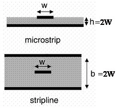
Characteristic impedance Z0 is a function of the transmission line's geometry and the properties of the dielectric material used. To accurately control impedance, these key factors must first be understood and quantified.
The calculation of characteristic impedance Z0 mainly depends on three core variables: trace width (W), dielectric thickness (H), and dielectric constant (ϵr).
1. Trace Width (W) and Dielectric Thickness (H): Trace width (W) directly determines the effective coupling area between the conductor and the reference plane. In the impedance calculation formulas, it is one of the most sensitive variables affecting Z0. Dielectric layer thickness (H) is equally crucial; it directly impacts the line's capacitance per unit length (C) and is a key parameter design engineers use to tune the target Z0 during stackup design.
2. Geometric Correction for Copper Thickness (T): In addition to W and H, copper foil thickness (T) cannot be ignored. Due to the inherent physics of chemical etching, the etchant not only removes copper vertically but also laterally undercuts the copper protected by the photoresist. This results in the actual trace cross-section being trapezoidal rather than an ideal rectangle. Therefore, T must be factored into precise Z0 calculations as it determines the average effective trace width. Ignoring this effect in high-precision scenarios can lead to a systemic underestimation of the impedance prediction.
The dielectric constant (ϵr), or Dielectric Constant (Dk), is a macroscopic representation of the substrate material's ability to store electric field energy and has a decisive influence on Z0. Dk is inversely related to characteristic impedance: a higher ϵr leads to larger effective line capacitance, thus resulting in a lower characteristic impedance Z0.
For precise control of high-speed PCB impedance, the frequency dependence of the Dk, known as the material's dispersion characteristics, must be considered. For signals operating at several GHz or higher, ϵr is not a fixed value; it tends to slightly decrease as frequency increases. This frequency dependence is known as dispersion characteristics.
For signals operating at frequencies above several GHz, the material's dispersion characteristics cause its dielectric constant to change with frequency, consequently affecting the stability of the effective dielectric constant (ϵeff) and the precision of impedance control. For example, traditional Polyimide (PI) material used in Flexible Printed Circuits (FPC) has a high Dk and Dissipation Factor (Df), leading to increased signal delay and loss at high frequencies. Furthermore, PI has a high moisture absorption rate. Since water has an extremely high Dk and Df, increasing moisture absorption in the substrate inevitably exacerbates signal delay and loss.
Therefore, high-precision designs must use the ϵr values provided by the material supplier at the actual operating frequency. Crucially, for extremely high-speed applications, design engineers need to select materials with low Dk and low Df characteristics, such as Liquid Crystal Polymer (LCP) or modified Polyimide (modified PI), based on the signal's operating frequency. This ensures stable and precise impedance across a broad bandwidth while minimizing signal loss.
Additionally, the stability of the material's ϵr itself, meaning its fluctuation with temperature and humidity changes, also indirectly affects the final impedance precision. Selecting materials with low Df and high ϵr stability is a prerequisite for achieving high-precision impedance control.
The Solder Mask is one of the final steps in PCB manufacturing, and its presence is particularly significant for Microstrip structures. In a Microstrip configuration, the trace is exposed to a dual dielectric environment: air and the solder mask. The solder mask covers the trace surface, and its own thickness (M) and dielectric constant (ϵr,mask) alter the transmission line's effective dielectric constant (ϵeff).
If the design engineer fails to account for the solder mask's influence in the Z0 calculation, particularly when the mask layer is thick, a systemic deviation between the predicted and actual impedance values will occur. Hence, in precise impedance models, solder mask thickness and its electrical parameters are mandatory secondary correction factors.
> Recommend reading: Solder Mask Material: Everything You Need to Know - NextPCB
Table II: Key Design and Manufacturing Parameters Affecting PCB Characteristic Impedance (Z0)
| Parameter Name | Symbol | Unit | Design Stage Influence | Source of Manufacturing Variation |
|---|---|---|---|---|
| Dielectric Constant | ϵr | Dimensionless | Dielectric material selection (substrate) | Material batch and curing rate inconsistency, leading to Dk fluctuation across the board and batches (Δϵr) |
| Dielectric Thickness | H | μm | Core parameter in impedance calculation formula | Thickness change (ΔH) caused by uneven resin flow, curing shrinkage, or press pressure variation during the lamination process |
| Trace Width | W | μm | Directly determines impedance | Etching undercut and uniformity ΔW, for example, trace width variation caused by uneven photoresist protection or differences in etching time |
| Copper Thickness | T | μm | Affects effective width and loss | Initial copper foil thickness and plating deposition tolerance, affecting the final conductor cross-sectional area |
| Solder Mask Thickness | M | μm | Affects Microstrip effective dielectric environment | Solder mask uniformity from screen printing or spraying, affecting localized thickness |
Achieving high-precision impedance control of ±5% requires the core challenge of constraining manufacturing variability (tolerance) within an extremely narrow range. Impedance precision is essentially a direct reflection of the level of tolerance management in the manufacturing process.
Among all manufacturing factors, trace width variation (ΔW) is the dominant contributor to characteristic impedance tolerance, especially in the context of modern PCB designs trending towards finer lines.
Line width variation lies in the inherent physics of the chemical etching process. During manufacturing, copper material protected by photoresist is chemically eroded. While the main direction of erosion is vertical, lateral erosion (Side Etch) is unavoidable. This lateral etching causes the final trace width to be smaller than the designed photoresist pattern, resulting in a trapezoidal cross-section.
The sources of variation leading to ΔW are complex and interconnected, including: the thickness and uniformity of the photoresist coating, the concentration and temperature of the developer, the chemical activity of the etchant, and the etching time. A deeper challenge lies in the non-uniformity of the etching process itself. Within a single PCB panel, variations in etchant flow rate, temperature distribution, and chemical consumption can lead to differing etch rates across different areas, directly resulting in ΔW inconsistencies across the board. Precise control over these complex chemical and physical parameters is key to achieving high-precision ΔW control.
The challenge of trace width control peaks when faced with high aspect ratio structures. When design requirements simultaneously demand thicker copper layers (T ≥ 35 μm) and narrower trace widths (W ≤ 100 μm), the manufacturing difficulty increases sharply. This high Aspect Ratio (T/W) structure complicates side etch control, significantly increasing the uncertainty of ΔW.
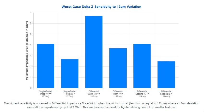
In high T/W structures, the surface area of the conductor sidewalls increases relatively, and it becomes more difficult for the etchant to reach the bottom sidewall. Any slight fluctuation in etching process parameters will have a larger percentage impact on the amount of side etch. This means the process control required to maintain the target W must be elevated to the extreme. For example, it may require advanced Pulse Plating technology to achieve denser copper layers with finer grain structures, or rely on more precise exposure equipment to ensure sharp photo-pattern boundaries. Manufacturers must use stringent Statistical Process Control (SPC) to stabilize all critical parameters affecting the etch rate, including chemical concentration, temperature, and solution dwell time, thereby ensuring ΔW is constrained to the minimum possible range to meet high-precision controlled impedance requirements.
However, the impedance precision challenge is not limited to the horizontal dimension (trace width W). In the challenge of manufacturing precision, in addition to the etching process, tolerance in the lamination process is also a major factor contributing to impedance inconsistency, primarily manifested as dielectric thickness variation (ΔH). Dielectric thickness variation (ΔH) is an unavoidable source of error during the lamination of multilayer boards. When the prepreg is cured under high temperature and pressure, the resin flow significantly influences the final thickness. Resin content, cure temperature profile, press pressure, and stackup structure all affect the final dielectric thickness.
> Rercommend reading: Choosing High-Speed PCB Stackups from 4 to 10 Layers
Although the dielectric thickness H is a target value in the design, the ΔH generated in actual manufacturing must be included as an independent error source in the total impedance tolerance calculation model. For high-layer count and High-Density Interconnect (HDI) designs, controlling ΔH becomes even more difficult as it involves complex resin fill and thickness shrinkage models.
Beyond geometric tolerances in manufacturing, the intrinsic properties of the substrate materials also exhibit variability. The material's dielectric constant (ϵr) is not ideally constant. Even for specified high-performance substrate materials, small differences in ϵr can exist between different batches, or even at different locations on the same panel. This variation primarily stems from slight fluctuations in resin content, inconsistencies in fiberglass weave density, and inherent tolerance in the degree of cure.
For high-speed designs aiming for ±5% precision, the error introduced by this Δϵr, while typically smaller than geometric tolerance, is still part of the systemic error budget. Therefore, materials with extremely low ϵr tolerance must be selected (such as low Dk/Df materials with more stable glass cloth content and uniform weave structure), and the manufacturer should provide detailed material batch consistency reports to ensure the reliability of the design and manufacturing models.
Achieving high-precision impedance control requires shifting from qualitative description to rigorous quantitative analysis, using mathematical models to predict and manage the superposition of errors.
Characteristic impedance Z0 is a complex function of multiple variables, including trace width W, dielectric thickness H, and dielectric constant ϵr. To quantify the extent to which each manufacturing variable influences the final Z0, a sensitivity analysis must be performed.
1. Sensitivity Analysis: Sensitivity analysis uses partial derivatives to quantify the impact (ΔZX) of a minor change (ΔX) in any variable X on Z0. The purpose of this formula is to quantify the influence of a minor variation in parameter X on the characteristic impedance Z0, described by the sensitivity coefficient:
ΔZX = (∂Z0 / ∂X) * ΔX
Here, (∂Z0 / ∂X) is the parameter's Sensitivity Coefficient. It represents how much the characteristic impedance Z0 will change for every unit change in the parameter X (such as trace width W or dielectric thickness H). A higher sensitivity coefficient means that a minor manufacturing tolerance (ΔX) for that parameter will lead to a larger impedance fluctuation (ΔZX). Therefore, manufacturers must exercise stricter control over highly sensitive parameters.
2. Statistical Superposition Model (RSS Method): Since manufacturing errors like ΔW, ΔH, and Δϵr are typically considered independent random variables, the total impedance tolerance (ΔZtotal) should not be calculated using a worst-case analysis (simple algebraic summation). Instead, it must be superimposed using a statistical method: the Root Sum Square (RSS). This model more accurately reflects the probability distribution of errors in actual production:
ΔZtotal = √((ΔZW)2 + (ΔZH)2 + (ΔZϵr)2 + (ΔZT)2 + ...)
This statistical superposition model is the core tool for predicting and controlling total impedance tolerance.
The table below precisely illustrates the total impedance tolerance (ΔZtotal) quantification model, clarifying how each variation factor is converted into a contribution to the total tolerance via the sensitivity coefficient:
| Variable Factor | Symbol | Tolerance/Variation | Sensitivity Coefficient (Definition) | Contribution to Total Tolerance |
|---|---|---|---|---|
| Trace Width | W | ΔW (Etching Tolerance) | (∂Z0 / ∂W) | ΔZW = (∂Z0 / ∂W) * ΔW (Actual manufacturing deviation of trace width multiplied by its sensitivity to impedance, one of the primary contributors to total tolerance) |
| Dielectric Height | H | ΔH (Lamination Tolerance) | (∂Z0 / ∂H) | ΔZH = (∂Z0 / ∂H) * ΔH (Actual manufacturing deviation of dielectric thickness multiplied by its sensitivity to impedance) |
| Dielectric Constant | ϵr | Δϵr (Material Tolerance) | (∂Z0 / ∂ϵr) | ΔZϵr = (∂Z0 / ∂ϵr) * Δϵr (Material's inherent tolerance multiplied by its sensitivity to impedance) |
| Total Tolerance | Ztotal | ΔZtotal | N/A | √((ΔZW)2 + (ΔZH)2 + (ΔZϵr)2 + ...) |
Quantitative analysis shows that in most standard and miniaturized PCB stackups, due to the relatively large inherent tolerance ranges of the etching and lamination processes, the contribution of trace width (W) and dielectric height (H) to the total impedance tolerance is usually much higher than that of the dielectric constant (ϵr). This implies that even with the most advanced low-Δϵr materials, high-precision impedance targets cannot be met if geometric dimensional control is poor.
This quantitative result reveals a critical engineering strategy: design robustness against manufacturing tolerance.
Since the manufacturing processes (e.g., etching equipment and chemistry) determine an absolute range for ΔW and ΔH that is difficult to fundamentally change, the designer's best strategy is to adjust the design values of W and H to minimize the sensitivity coefficient of the impedance to these parameters.
For example, for a given 50Ω structure, if the design allows, choosing a wider trace (W) can effectively absorb the fixed value of manufacturing tolerance. Assume the etching error ΔW is a fixed 10 μm. If the target trace width is 100 μm, ΔW accounts for 10% of the width; but if the target trace width is 200 μm, ΔW accounts for only 5%. By choosing a wider trace, the design significantly lowers the impedance's sensitivity to changes in W (∂Z0 / ∂W), thereby effectively reducing the relative contribution of ΔZW and making it easier for the final ΔZtotal to meet high-precision requirements.
Advanced impedance control relies not only on precise theoretical models but also on close collaboration between design and manufacturing processes and a rigorous quality assurance system.
1. Simulation and Prediction: At the start of PCB design, precise 2D/3D electromagnetic field solvers must be used to model the stackup. More importantly, the design must incorporate actual process tolerance data (including the statistical range for ΔW and ΔH) provided by the target manufacturer to run predictive sensitivity analyses. Through this predictive simulation, engineers can determine whether ΔZtotal can meet the ±5% high-precision target under the given manufacturing capability, allowing for stackup optimization during the design phase.
2. Etch Compensation Strategy (EC): Since side etch is a systemic deviation, high-precision manufacturing must incorporate an etch compensation strategy. For instance, if a manufacturer's historical data indicates that their etching process typically results in 17 μm of side etch, the design engineer must pre-enlarge the trace width by 34 μm (17 μm on each side) in the Gerber files to ensure the final etched conductor width closely matches the target value, thus eliminating systemic deviation.
The key to high-precision manufacturing is minimizing variability by transforming systemic deviations into predictable random ones and controlling them tightly.
1. Fine-Tuning Etching Control: To minimize ΔW, manufacturers must use automated and closed-loop control systems to monitor key parameters influencing the etch rate in real-time, including the etchant's specific gravity, density, temperature, and chemical activity. Only through continuous Statistical Process Control can the consistency of ΔW between batches and across the panel be guaranteed. Leading manufacturers like NextPCB manage etching tolerance through strict SPC processes to meet customers' demands for impedance precision.
2. Lamination Consistency: Controlling dielectric thickness variation (ΔH) is critical for lamination. This requires the manufacturer to precisely control the resin content of the prepreg and optimize the press machine's temperature curve and pressure parameters. For high-precision impedance boards, higher pressing pressures and more stable temperature controls are typically employed to minimize thickness fluctuations caused by resin flow, ensuring the uniformity of the dielectric thickness across the panel.
Time Domain Reflectometry (TDR) testing is the gold standard and an industry-required test method for verifying PCB controlled impedance compliance.
1. TDR Operating Principle and Authority: TDR works by launching an extremely fast rising edge pulse onto the transmission line and measuring the reflected energy along the path. If the impedance is perfectly matched, reflections are minimal; if an impedance mismatch exists, a reflection occurs. TDR displays the impedance profile along the transmission line on a time-domain graph. Qualified manufacturers must perform TDR testing on production samples, not only to verify the final product against the target tolerance but, more importantly, because TDR data provides a critical feedback loop.
2. Quality Loop and Reliability: This process, based on physical measurement and data calibration, is direct evidence of reliability requirements. The TDR test reports provided by the manufacturer are the most authoritative proof for customers to verify that high-precision impedance requirements have been met.

Achieving high-precision controlled impedance (e.g., ±5%) is a complex system engineering endeavor that successfully integrates design theory with manufacturing practice. Success hinges on two core elements: first, the design engineer must minimize the sensitivity of the characteristic impedance Z0 to changes in geometric dimensions; and second, the manufacturer must use advanced Statistical Process Control to strictly constrain manufacturing tolerance (particularly ΔW and ΔH).
Try NextPCB Stackup and Impedance Calculator
1. Geometric Tolerance is the Dominant Factor: Although material properties are crucial, in the statistical superposition model (RSS) for impedance tolerance, variations in trace width (ΔW) and dielectric thickness (ΔH) are typically the main contributors to the total impedance tolerance (ΔZtotal). The core of achieving high-precision impedance control lies in high-precision etching and lamination process management.
2. The High Aspect Ratio Challenge: For designs requiring thick copper (T ≥ 35 μm) and fine lines (W ≤ 100 μm), manufacturing difficulty increases sharply because the high T/W aspect ratio makes side etch control extremely challenging. Manufacturers must demonstrate their capability to handle such high-difficulty structures.
3. Model Precision: Advanced impedance control must rely on quantitative analysis that integrates design parameters (W, H, ϵr, T, M) and their manufacturing tolerances (ΔW, ΔH, Δϵr) into a statistical superposition model to accurately predict the final impedance range.
NextPCB positions itself as a specialized, reliable multilayer PCB manufacturer, offering a one-stop solution encompassing PCB manufacturing, assembly, and prototyping. Their core impedance control services are designed to meet the rigorous signal integrity requirements of cutting-edge technologies, including USB4, PCIe Gen 6, 5G, Wi-Fi 7, and mmWave radar.
NextPCB capabilities extend beyond standard boards, supporting:
NextPCB is committed to providing easy, cost-effective, and repeatable impedance control solutions, understanding that close client-manufacturer synergy is essential for maximizing high-speed performance.
For customers seeking high-precision controlled impedance services, it is recommended that when selecting a PCB manufacturer, they not only ask if controlled impedance service is offered but also deeply investigate the following key capabilities:
Achieving Zero Defect Impedance Control
Achieving tight impedance tolerances (+/- 5% or better) is a complex, multi-variable challenge. It requires stringent process control over geometry and a robust feedback system for material properties like DK. PCB manufacturers must utilize advanced TDR measurement and back-calculation techniques to ensure reliable signal integrity for the next generation of high-speed electronics. For world-class fabrication expertise in controlled impedance PCBs, rely on NextPCB.

Still, need help? Contact Us: support@nextpcb.com
Need a PCB or PCBA quote? Quote now

