

 NextPCB Capabilities
 PCB Assembly
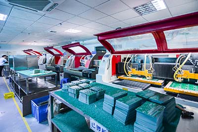
 Layer Buildup
 SMD-Stencils
 PCB Design-Aid & Layout
 Mechanics
 Surface
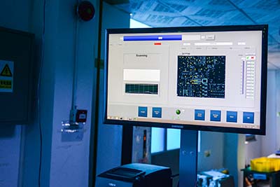
 Quality
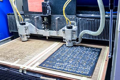
 Drills & Throughplating
 Factory & Certificate


-
-
-
-
-
-
-
-
-
-
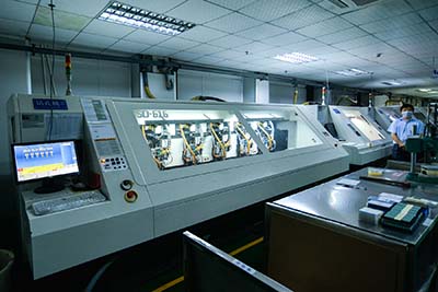
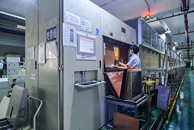
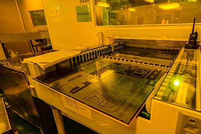
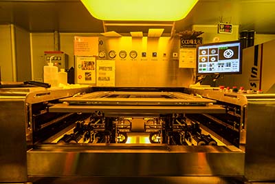
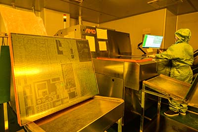
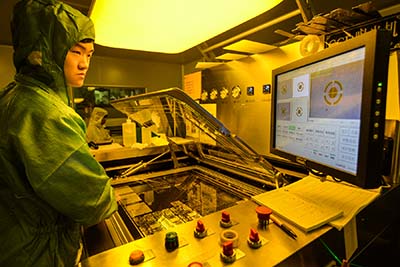
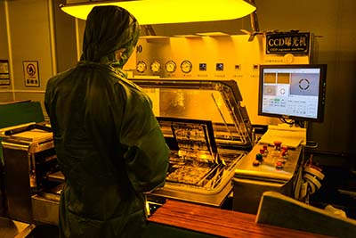
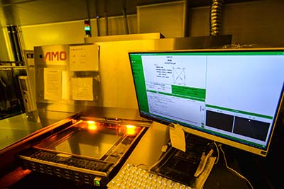
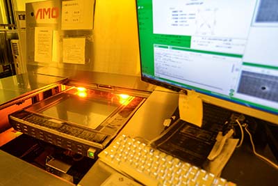
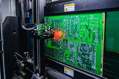
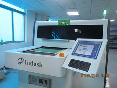
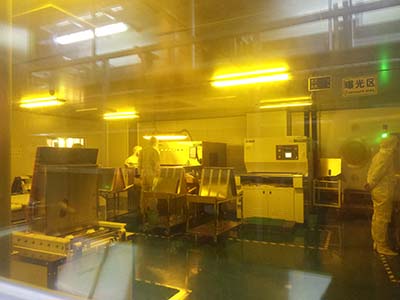
Light painting operation--photographing system
The process is as shown below: (PCB/LCD design)-->(CAM system)-->(Gerber file)
4598 1 0 Shares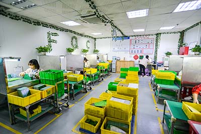
-
-
-
-
-
-
-
PCB design skills based on GENESIS2000 software (2)
Part 6-12
8427 6 0 Shares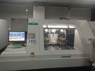
-
PCB design skills based on GENESIS2000 software (1)
Part 1-5
6572 1 0 Shares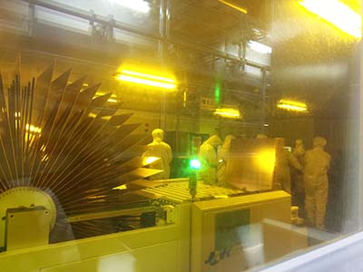
-
-
Categories
Recommended Article:
- IRLB3034 Pinout, Datasheet & Equivalents: The Complete Reference
- Raspberry Pi 5 Pinout: Full GPIO Reference & What RP1 Changes
- Raspberry Pi 4 Pinout: Full GPIO Reference & BCM2711 Details
- Raspberry Pi Pico GPIO Pinout: Complete Pin Reference & Peripheral Map
- Raspberry Pi GPIO Pinout: The Complete Guide (Pi 5, Pi 4 & Pico)
- 78H24 Pinout Explained: What It Really Is (and What to Use Instead)
- Rogers 5880 (RT/duroid 5880): Dielectric Constant & Datasheet Guide
- Circuit Boards China: PCB Fabrication Guide 2026
- 5-Band Resistor Color Code: How to Read It (Free Calculator Inside)
- What Is a Microvia? Types, Design Rules & HDI Guide