

 NextPCB Capabilities
 PCB Assembly
 Layer Buildup
 SMD-Stencils
 PCB Design-Aid & Layout
 Mechanics
 Surface
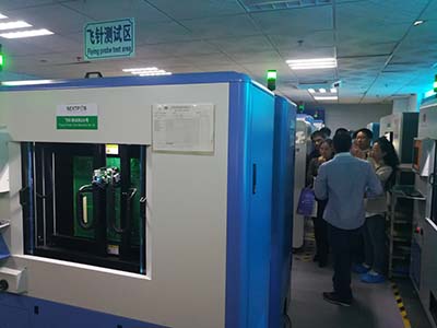
 Quality
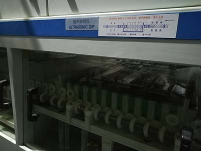
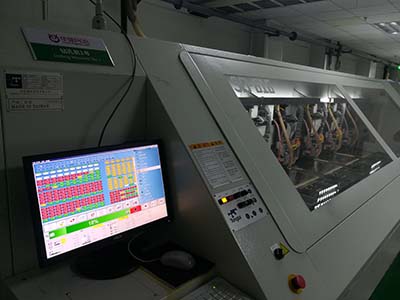
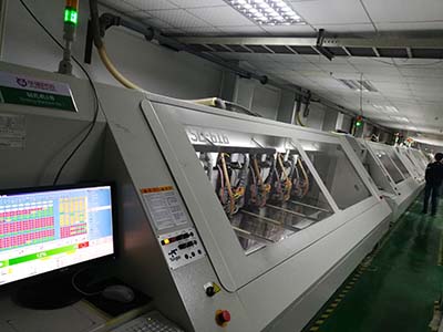
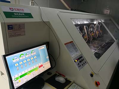
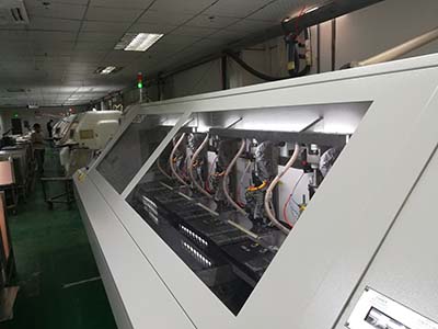
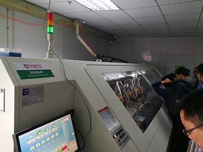
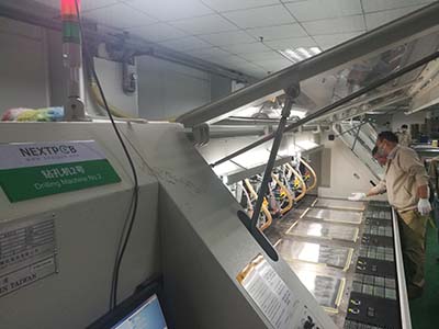
 Drills & Throughplating
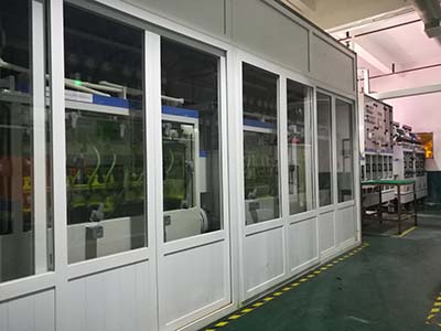
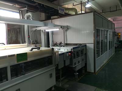
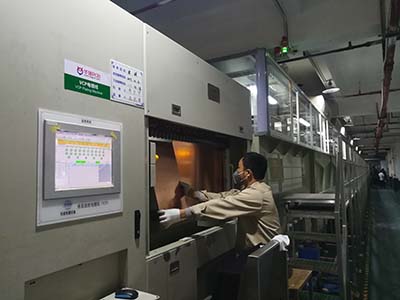
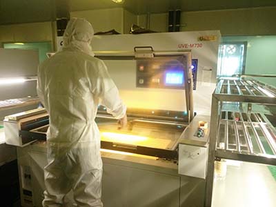
 Factory & Certificate


-

-
-
-
Correct differential pair routing method in Altium 9
How to define differential pairs in the schematic
7923 6 0 Shares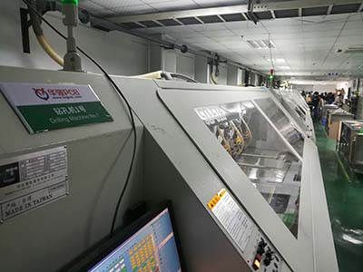
-
-
-
-
-
-
The golden rule that PCB design never changes
10 Rules
4476 1 0 Shares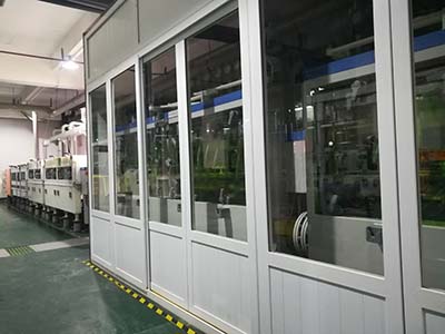
-
PCB design technology
PCB design techniques have an impact on the following three effects:
4711 1 0 Shares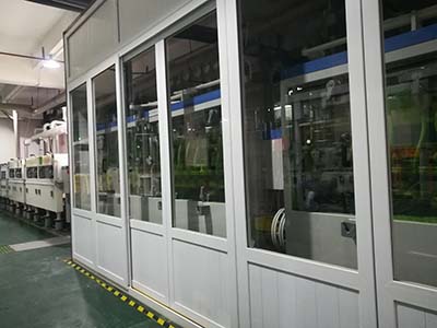
-
-
-
-
PCB layout design view elements
55 elements
4701 1 0 Shares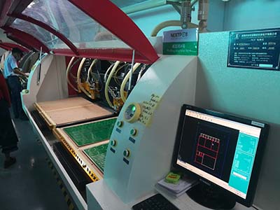
-
-
-

-
-
Categories
Recommended Article:
- Toroidal vs Drum Core vs Shielded SMD Inductor: Choosing the Right Form Factor
- How to Place Inductors on a PCB: Orientation, Spacing and EMI Rules for DC-DC Converters
- Shielded vs Unshielded Inductors: EMI Impact and PCB Placement Best Practices
- Common Mode Choke: How It Works, PCB Layout Rules and Differential Pair Applications
- Ferrite Bead vs Inductor: When to Use Each for EMI Filtering in PCB Design
- Power Inductor Selection Guide: Inductance, DCR & PCB Footprint
- MLCC Piezoelectric Effect: Acoustic Noise, Microphonics and How to Mitigate in PCB Design
- Bulk vs Decoupling Capacitor: The Three-Tier Capacitor Strategy
- ESR and ESL in Capacitors: What They Mean and Why They Matter in PCB Power Integrity
- Film Capacitor vs Ceramic Capacitor: Applications, Trade-offs and PCB Layout Considerations