
 NextPCB Capabilities
Printed Circuit Boards
NextPCB Capabilities
Printed Circuit Boards
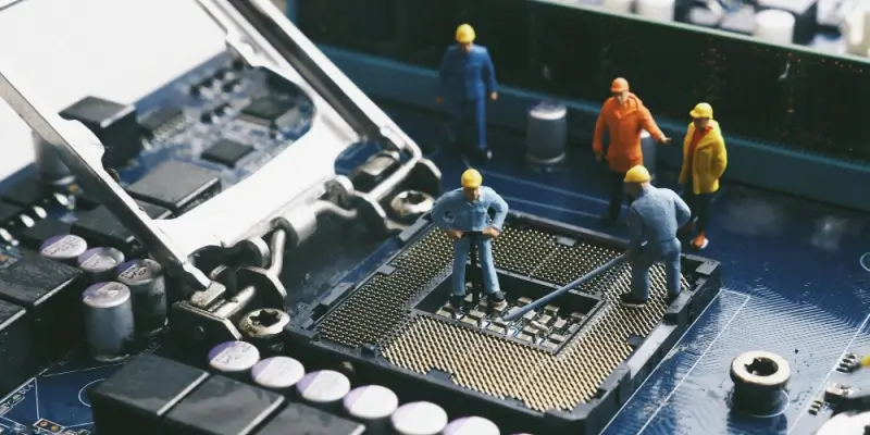
 PCB Assembly
 Layer Buildup
 SMD-Stencils
 PCB Design-Aid & Layout
 Mechanics
 Quality
 Drills & Throughplating
 Factory & Certificate
 PCB Assembly Factory Show
Certificate
PCB Assembly Factory Show
Certificate
Support Team
Feedback:
support@nextpcb.com


Introduction
The Printed Circuit Board (PCB) assembly services market is a foundation of modern electronics manufacturing. This process involves mounting and soldering components, such as integrated circuits, resistors, and capacitors, onto a circuit board according to a precise design layout. PCB assembly encompasses a wide range of applications, including smartphones, wearable devices, industrial automation, and electric vehicles. Global Market Insights reports that the PCB assembly market was valued at roughly USD 90 billion in 2023 and is projected to grow at a compound annual growth rate (CAGR) of 5%, reaching an estimated USD 145 billion by 2032. This growth is driven not only by rising demand for consumer electronics but also by increasing adoption of high-density interconnect (HDI) technologies and automated assembly processes that improve precision and reliability.
A pivotal trend shaping the market is the transition from 200 mm to 300 mm semiconductor wafers. Larger wafers increase die yield and reduce per-unit costs, yet they introduce challenges in component handling, inspection, and assembly processes. Understanding these technical implications is important for Original Equipment Manufacturers (OEMs), engineers, and PCB assembly service providers seeking efficiency, cost optimization, and alignment with the evolving semiconductor landscape. This article examines market dynamics, regional segmentation, technology trends, and wafer-size impacts to provide a comprehensive guide for industry stakeholders.
>Read & Download full PCB Assembly Guide.
The global PCB Assembly Services market was valued at USD 90 billion in 2024, with the Asia Pacific region capturing the largest share. According to a report by Meticulous Research published on PR Newswire, the region is expected to account for over 60% of the PCBA market in 2025. This region boasts a robust manufacturing base, particularly in countries like China, Japan, South Korea, and Taiwan, which are equipped with advanced infrastructure, skilled labor, and efficient supply chains.
China, in particular, continues to reinforce its dominance in the Asia Pacific PCB market. In 2024, China's mainland PCB industry attained a global market share of 32.8%, with a projected output value of $26.79 billion. This growth is a result of strong government support and high demand from key sectors like electric vehicles and AI.
Leading manufacturers in China, such as NextPCB, are driving technological advancements, producing prototypes with up to 120 layers and mass-producing boards with up to 68 layers. This rapid shift toward high-end, high-density PCBs underscores China’s strategic role in shaping both regional and global market trends. NextPCB leverages cost-effective manufacturing, advanced supply chain networks, and proximity to high-growth electronics markets, providing them with a strategic edge and significantly influencing global market dynamics.
Positioned among the top-tier assembly providers, NextPCB offers advanced capabilities, including up to HDI boards, rigid-flex, and metal-core PCBs, with certifications such as IATF 16949, ISO 9001/14001, UL, RoHS, and REACH. Its expansive manufacturing footprint, including three large factories and 27 high-precision SMT lines, ensures rapid turnaround, exceptional quality, and responsiveness across Asia and beyond.
Several technological advancements are actively redefining the PCB assembly landscape, improving efficiency, precision, and scalability:
The market for high-density interconnect (HDI) printed circuit boards is seeing a marked shift toward higher layer counts, with up to 32 layers becoming increasingly common in consumer electronics, automotive, and aerospace. This trend is driven by the demand for smaller, lighter devices that don't sacrifice functionality. The global High-Density Interconnect market, valued at USD 16.81 billion in 2023, is projected to grow at a 12.1% CAGR from 2024 to 2030, reaching approximately USD 37.39 billion. This data reflects the adoption of miniaturized, high-performance assemblies across multiple sectors.
Fan-out wafer-level packaging (FOWLP) and other advanced packaging technologies are gaining traction as cost-efficient solutions for achieving compact, high-performance designs in mobile devices and IoT applications. By supporting finer-pitch components and improving thermal management, these approaches minimize PCB footprint while boosting signal integrity and overall reliability. The global Fan-Out Packaging market is projected to grow from USD 3.43 billion in 2025 to USD 7.35 billion by 2030. This represents a robust CAGR of 16.5% over the forecast period, a clear indicator of the rising importance of package-level innovation in electronics manufacturing..
In PCB manufacturing, quality control is increasingly driven by advanced technologies such as Automated Optical Inspection (AOI), X-ray inspection, and AI-powered predictive analytics. Industry studies and research consistently demonstrate that these solutions enhance both accuracy and efficiency by automating inspection tasks and reducing the high false-positive rates commonly associated with manual checks. Findings from ResearchGate suggest that AI-based defect detection, utilizing computer vision and machine learning, can achieve detection accuracies exceeding 95%, representing a significant improvement over traditional methods.
NextPCB has fully embraced these trends. With high-precision SMT lines, integrated AOI, X-ray, and digital monitoring systems, and the capability to produce multi-layer HDI, rigid-flex, and metal-core PCBs, NextPCB ensures high yield, reduced defects, and rapid delivery, meeting the stringent demands of modern electronics OEMs.
The size of a semiconductor wafer plays a major role in determining production efficiency, cost-per-chip, and yield. Over the past three decades, the industry has steadily migrated from 100 mm wafers to 200 mm and 300 mm standards, with ongoing research into 450 mm formats.
The switch from 200 mm (8-inch) to 300 mm (12-inch) wafers enables a 2.25x increase in usable surface area, allowing manufacturers to fabricate significantly more chips per wafer. This scaling reduces the cost-per-die by up to 30%, even after factoring in higher equipment and process costs. According to a 2024 report, 300 mm wafers were expected to account for roughly 70% of global wafer production, primarily serving high-volume applications such as advanced processors, high-bandwidth memory, and power devices.
In 2023, China’s chip manufacturing capacity was set to grow 12% Year-over-Year to 7.6 million wafers per month (WSPM), with a further 13% increase in 2024 to 8.6 million WSPM. This strategic push strengthens China’s position in the global semiconductor supply chain and provides its PCB manufacturing sector, including NextPCB, with faster access to advanced chipsets for high-speed, high-density assemblies.
Larger wafers enable the production of high-performance ICs at lower costs. This, in turn, is driving demand for compact, high-layer-count PCBs in applications such as AI accelerators, electric vehicles, and 5G infrastructure. NextPCB’s SMT lines are optimized for fine-pitch component placement and high thermal-performance boards, ensuring compatibility with the latest chip packaging formats emerging from 300 mm fabs.
| Aspect | 200 mm Wafer | 300 mm Wafer |
| Wafer Diameter | 200 mm (8 inches) | 300 mm (12 inches) |
| Die Per Wafer | ~314 average (depending on die size) | ~706 average (2.25× surface area) |
| Yield | Lower, higher per-unit cost | Higher, cost-per-die reduced by up to 30% |
| Equipment Cost | Lower initial investment | 20–40% higher initial investment |
| Process Complexity | Less complex | More complex, requiring advanced process control |
| Material Utilization | Less efficient | More efficient, reduced waste |
The move from 200 mm to 300 mm wafers significantly increases production capacity, enabling nearly double the number of chips per wafer, while lowering cost per chip in high-volume manufacturing. However, it demands more advanced lithography, tighter process controls, and higher upfront equipment costs. NextPCB capitalizes on this trend with precision SMT lines designed for fine-pitch BGA, QFN, and chip-scale packages. Their experience handling HDI PCBs and thermally optimized substrates ensures engineers can integrate the latest semiconductor technology without redesign bottlenecks.
NextPCB leverages advanced engineering capabilities to stay ahead of rapid shifts in semiconductor technology and PCB assembly demands:
Our SMT lines handle ultra-fine pitches down to 0.25 mm, supporting complex ICs from 300 mm wafer production that enable higher transistor density and better performance-per-watt. Capable of stacking 8+ PCB layers with laser-drilled microvias for HDI designs, we meet the miniaturization needs of smartphones, wearables, and AI edge devices.
Supports low-loss laminates (e.g., Rogers, Isola) for high-frequency applications, critical for 5G and high-speed computing. Our reflow profiles are tuned for lead-free SAC305 and advanced package-on-package (PoP) assemblies, minimizing thermal stress while maximizing solder joint reliability.
Employs 3D Automated Optical Inspection (AOI) for detecting co-planarity issues in BGA packages, X-ray inspection for hidden solder joints, and in-circuit testing (ICT) for verifying functional performance. Processes comply with IPC-A-600 and IPC-A-610 Class 3 standards for mission-critical electronics.
With the industry moving from 200 mm to 300 mm wafers, NextPCB’s processes are calibrated to accommodate components with higher I/O counts, smaller geometries, and tighter tolerances. This ensures compatibility with AI accelerators, automotive-grade MCUs, and other high-complexity chipsets.
Offers everything from 24-hour quick-turn prototyping to fully automated high-volume production, supported by real-time tracking systems and engineering change order (ECO) management for rapid design iterations.
By combining precision manufacturing, material expertise, and strategic alignment with semiconductor advancements, NextPCB ensures your designs remain manufacturable, cost-efficient, and performance-optimized in a rapidly evolving market.
The PCB assembly market is entering a transformative phase, driven not only by rising demand in consumer electronics, automotive EVs, and AI-enabled devices but also by rapid technological evolution in semiconductor fabrication. By 2032, global PCB assembly revenue is projected to surpass USD 147 billion, with high-density interconnect (HDI) and mixed-technology boards leading growth.
For OEMs, success will increasingly depend on aligning with PCB providers who are themselves innovating, those adopting 300 mm wafer-compatible processes, AI-driven inspection, and advanced packaging techniques. Relying on legacy assembly methods risks misalignment with next-generation components, longer lead times, and higher defect rates.
NextPCB exemplifies the type of partner OEMs should seek. Its high-precision SMT lines, automated quality control, and HDI expertise ensure compatibility with the latest semiconductor trends. By continuously upgrading equipment and processes, NextPCB allows OEMs to integrate cutting-edge chips efficiently while maintaining performance, reliability, and rapid time-to-market.
OEMs that strategically partner with forward-looking PCB providers like NextPCB gain a competitive edge. They can confidently leverage emerging technologies, optimize cost-per-die from wafer transitions, and scale production without compromising quality. In today’s market, such alignment is no longer optional; it is essential for delivering next-generation electronic products.
The PCB assembly services market is on a trajectory of sustained growth, propelled by miniaturization, advanced packaging, and the semiconductor industry’s shift from 200 mm to 300 mm wafers. This transition delivers higher yields, improved cost-per-die, and greater integration density, but also imposes tighter design tolerances, higher component I/O counts, and stricter thermal management requirements for PCB assembly.
For OEMs, success in this environment requires not only awareness of these technical implications but also a manufacturing partner with the process capability, equipment precision, and materials expertise to handle them.
By integrating HDI fabrication, low-loss laminate support, automated quality control, and high-mix, high-volume scalability, NextPCB offers engineers a path to align seamlessly with industry trends, ensuring electronic products are manufacturable, reliable, and performance-optimized in the era of next-generation semiconductors.
About the Author
Abiola Ayodele: Broadcast Journalist & Tech Writer; Cooperate writer of NextPCB.
Specialize in technical writing, and editing, particularly in the areas of PCB design, semiconductors, cybersecurity, and emerging engineering technologies.
Still, need help? Contact Us: support@nextpcb.com
Need a PCB or PCBA quote? Quote now


 Surface

