
 NextPCB Capabilities
Printed Circuit Boards
NextPCB Capabilities
Printed Circuit Boards
 PCB Assembly
 Layer Buildup
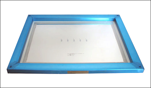
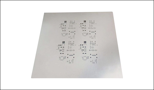
 SMD-Stencils
 PCB Design-Aid & Layout
 Mechanics
 Quality
 Drills & Throughplating
 Factory & Certificate
 PCB Assembly Factory Show
Certificate
PCB Assembly Factory Show
Certificate
Support Team
Feedback:
support@nextpcb.com


Particular efficiency problems associated with solder paste and also stencils are:
Throughout the print cycle, as the squeegee blade takes a trip throughout the stencil, solder paste loads the stencil aperture. Throughout the board/stencil splitting upcycle the paste launches to the pads on the board. Preferably, all the paste that loaded the aperture throughout the print procedure needs to have launched from the aperture wall surfaces and also moved to the pad on the board, creating a full solder block. Nevertheless, this transfer quantity depends upon the element proportion as well as the location proportion of the aperture.
As an example, with a location of the pad above two-thirds the location of the within the aperture wall surface, the paste can accomplish a launch of much better than 80%. This implies lowering the stencil density or enhancing the aperture dimension can offer a much better paste launch with the exact same location proportion.
The capacity of the solder paste to launch from the aperture wall surfaces of the stencil additionally depends upon the coating of the aperture wall surfaces. With electropolished and/or electroplated laser-cut apertures, the paste transfer effectiveness enhances. Nonetheless, the transfer of solder paste from the stencil to the PCB additionally depends upon the bond of the paste to the aperture wall surfaces of the pattern and also on the bond of the paste to the pad on the PCB. For a great transfer the last needs to be better, which suggests the printability depends upon the proportion of the pattern wall surface location to the open face location while neglecting small impacts such as the draft angle of the wall surface as well as its roughness.
The positional as well as dimensional precision of the solder block published on the PCB pad depends upon the top quality of the moved CAD information, the modern technology and also approaches utilized to make the stencil, and also the temperature level of the pattern throughout its usage. Additionally, the positional precision additionally relies on the positioning approaches made use of.
Framed Stencils are the best kind of laser-cut stencils readily available and also are developed for high-volume screen-printing throughout manufacturing runs. These are completely installed in a stencil framework with a mesh boundary firmly extending the stencil aluminum foil tight in the structure. Framed stencils with smooth aperture wall surfaces are advised for Micro BGAs as well as for elements with 16 Mil pitch and also listed below. Framed stencils supply the most effective positional as well as dimensional precision when made use of under-regulated temperature level problems.
For brief runs or model PCB setting up, frameless stencils use optimal solder paste quantity control. They are made to collaborate with a stencil tensioning system, which are recyclable stencil frameworks such as global structures. As the stencils are temporarily glued right into a framework, they are considerably less expensive than framed stencils as well as occupy significantly reduced storage area.
For attaining excellent printing results with a stencil, a selection of elements should develop an appropriate mix. These consist of:
Still, need help? Contact Us: support@nextpcb.com
Need a PCB or PCBA quote? Quote now


 Surface


grenna
Solder paste is commonly used to create electrical connections and mechanical bonds between printed circuit board pads and surface mount devices, such as resistors and capacitors. It is made up of powdered solder in a flux paste.