
 NextPCB Capabilities
Printed Circuit Boards
NextPCB Capabilities
Printed Circuit Boards
 PCB Assembly
 Layer Buildup
 SMD-Stencils
 PCB Design-Aid & Layout
 Mechanics
 Quality
 Drills & Throughplating
 Factory & Certificate
 PCB Assembly Factory Show
Certificate
PCB Assembly Factory Show
Certificate
Support Team
Feedback:
support@nextpcb.com


Introduction:
In this era of universal connectivity, communication between devices is no longer a plot from a science fiction movie. From the smartwatch on your wrist (Device A) to the smartphone in your pocket (Device B), the Internet of Things (IoT) is quietly connecting our lives, enabling seamless data exchange.
Behind this digital revolution, the Printed Circuit Board (PCB) and its assembly (PCBA) are the unsung heroes of every exceptional IoT device. From the TV we use to watch rockets launch, to the rockets themselves, PCBs are in almost every electronic product. It's safe to say that without PCBs, there would be no IoT as we know it today.
This article delves into the critical role of PCBs in IoT product development and shares how NextPCB's professional manufacturing services can help you take your innovative ideas from prototype to mass production.
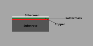
A traditional Printed Circuit Board (PCB) serves as the "home" for electronic components, physically holding and electrically connecting them via conductive pathways. A PCB is typically composed of four main layers:
Substrate: This is the "skeleton" of the PCB, providing structural support for all components and traces. It acts like the foundation of a house, with all other layers built upon it.
Copper Layer: A thin layer of copper foil is laminated onto the substrate. During manufacturing, these foils are etched to form conductive traces or "circuits," allowing electricity to flow from one component to another.
Solder Mask: This is a polymer coating, usually green, that lies on top of the copper layer. Its primary function is to insulate the copper traces, preventing them from shorting during the soldering process.
Silkscreen: This is the top-most layer, printed with white ink. It's used to add component names, numbers, logos, and symbols to the board, making it easier for engineers to identify and assemble components.
When a bare PCB is brought to life—by having all relevant electronic components correctly installed—it becomes a fully functional Printed Circuit Assembly (PCA). This process of "clothing" the bare board is known as PCB Assembly (PCBA).
> Recommend reading: IoT Development From Concept to Production: Prototyping & Best Practice
The manufacturing process for a PCB consists of two key steps:
Board Fabrication: This is the initial process of creating the bare PCB itself, which involves etching the copper layers, drilling holes, and applying the solder mask.
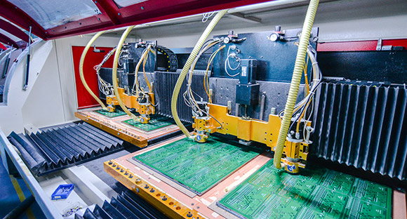
PCB Assembly (PCBA): This is the second step in the manufacturing process, where all components like resistors, capacitors, and chips are soldered and mounted onto the bare board, turning it into a working electronic module. > PCB Assembly Capabilities | Quick-Turn Prototype to Volume Production
The rise of the Internet of Things has brought unprecedented challenges and opportunities to the PCB manufacturing and assembly industry. To meet the demanding requirements of IoT devices for low power consumption, compact size, and high flexibility, PCB technology has been continuously evolving.
Take a smart wristband or fitness tracker as an example; it needs to integrate numerous functions in an extremely limited space. Traditional PCBs can no longer meet this demand. As a result, the PCB industry has introduced two revolutionary technologies:
High-Density Interconnect (HDI) PCBs: As the name suggests, HDI PCBs achieve a higher wiring density, smaller vias, and narrower traces, allowing more components to be integrated onto a tiny board space. For compact IoT products, HDI PCBs efficiently utilize space, significantly reducing product cost and volume.
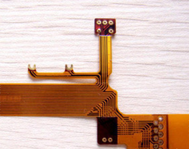
Flexible PCBs (Flex PCBs): Made with a bendable substrate, flexible PCBs can conform to various irregular shapes and spaces. This makes them an ideal choice for wearables, implantable medical devices, and other IoT products that require a high degree of flexibility.
For hybrid needs, rigid-flex PCBs combine rigidity with dynamic flex zones.
If you're weighing trade-offs, this explainers help: Flexible PCB—Ultimate Guide
By combining HDI and flexible PCB design approaches, manufacturers can help clients create smaller, lighter, and more innovative IoT products without compromising on performance.
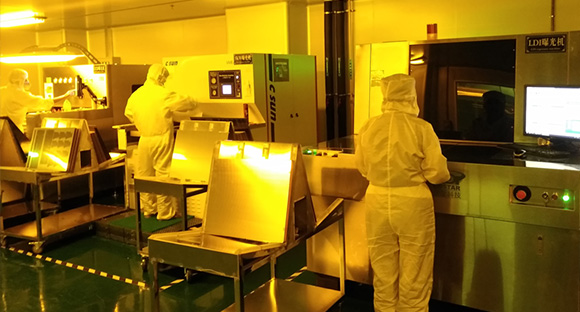
As a PCB manufacturing service provider with over 15 years of experience, NextPCB understands the critical role of high-quality PCBs in the success of IoT products. We not only offer exceptional PCB manufacturing services but are also equipped with advanced quality control tools like Automated Optical Inspection (AOI), X-ray testing, and multi-functional testing to ensure every board meets the highest standards.
With numerous quality certifications including IATF16949, ISO 9001, ISO 14001, UL, RoHS, CQC, and REACH, we are committed to providing reliable, cost-effective, and fast-turnaround PCBA services for your IoT projects.
Choose NextPCB to bring your innovative concepts to life with professional quality and speed.
See IoT Projects at NextPCB:
> KiCad 9: Design & assemble an ESP32 IoT 4-layer PCB
> Build Long-Range IoT Networks with Free RFM69HCW Prototypes-NextPCB Accelerator #12
> What the IoT Startups should know When Selecting IoT Hardware Partners

Still, need help? Contact Us: support@nextpcb.com
Need a PCB or PCBA quote? Quote now


 Surface

