
 Surface


Julia Wu - Senior Sales Engineer at NextPCB.com

 NextPCB Capabilities
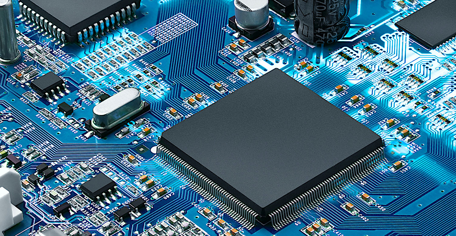
Printed Circuit Boards
NextPCB Capabilities
Printed Circuit Boards
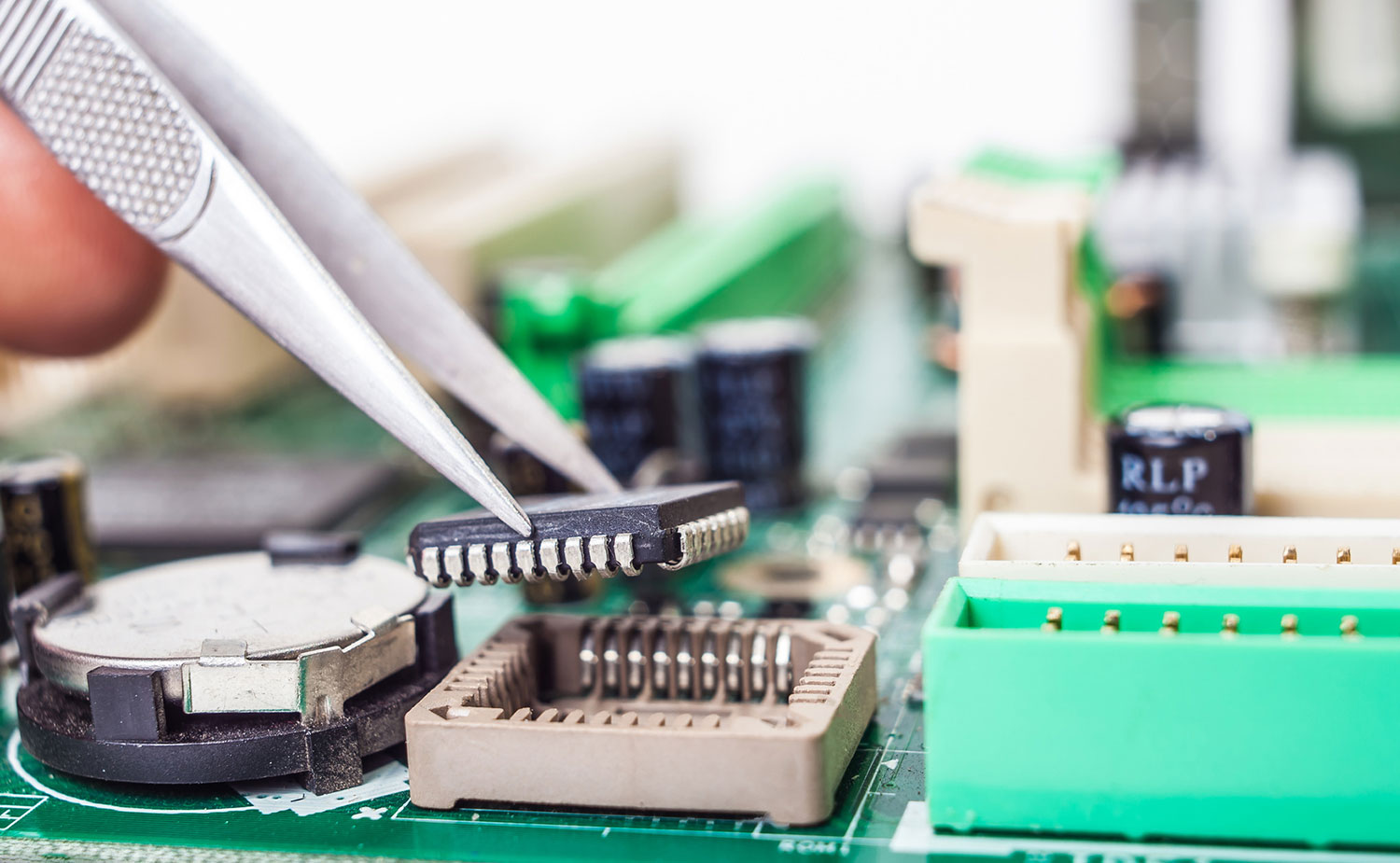
 PCB Assembly
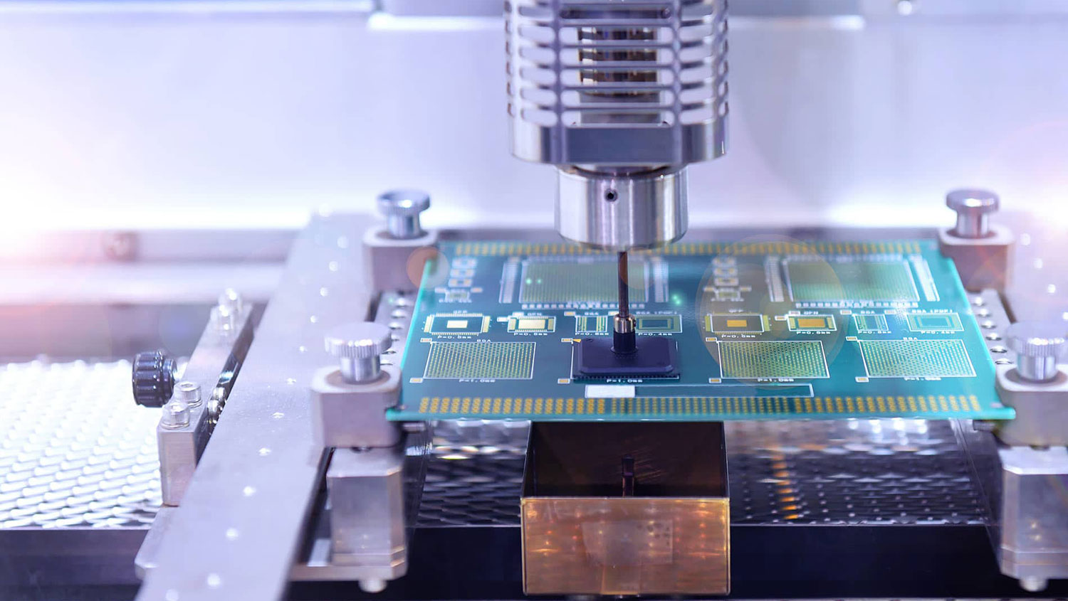
 Layer Buildup
 SMD-Stencils
 PCB Design-Aid & Layout
 Mechanics
 Quality
 Drills & Throughplating
 Factory & Certificate
 PCB Assembly Factory Show
Certificate
PCB Assembly Factory Show
Certificate
Support Team
Feedback:
support@nextpcb.com


Before diving into the technical engineering of integrated circuit (IC) substrates, hardware developers and procurement managers must understand the current macroeconomic forces shaping board availability and pricing. As we move deeper into 2026, the IC substrate landscape is experiencing a profound paradigm shift.
The explosive demand for high-speed data transmission, driven by generative AI, large language models, and 2.5D/3D advanced packaging architectures, has turbocharged the need for high-end ABF (Ajinomoto Build-up Film) substrates. Leading substrate like Unimicron Technology have explicitly noted that premium ABF substrates required for AI applications are aggressively leading the market's recovery, effectively pulling the sector out of its post-pandemic inventory slump.
However, this rapid demand resurgence brings new friction. A persistent shortage of specialized fiberglass and critical base resins in 2026 has tightened the supply chain. Consequently, manufacturers like Unimicron have begun raising substrate prices to offset raw material costs and capacity constraints. For electronics engineers and procurement teams, this means that optimizing your board design for manufacturability (DFM) and partnering with an agile PCB manufacturing partner is more critical than ever to control costs and secure reliable lead times.
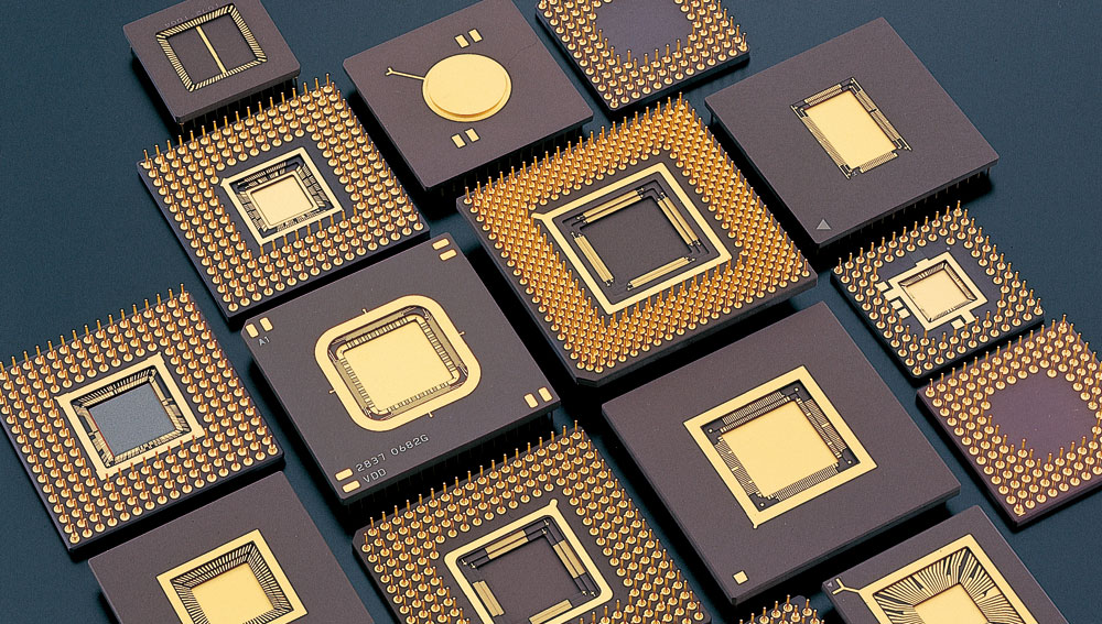
At its core, an IC package substrate is the crucial base material that bridges the gap between a microscopic semiconductor die (the bare chip) and the macroscopic printed circuit board (PCB). The evolution of modern integrated circuit types, such as Chip-Scale Packages (CSP) and Ball Grid Arrays (BGA), rendered traditional lead-frame packaging insufficient. These high-density silicon chips require novel, ultra-dense package carriers—the IC substrate.
Unlike a standard motherboard, the substrate is an intermediate component that performs several highly specialized engineering functions:
Standard printed circuit boards simply cannot achieve the miniaturization required for direct chip attachment. IC substrates look like PCBs but operate on entirely different scales of precision. When designing or sourcing an IC carrier, you will encounter the following typical specifications:
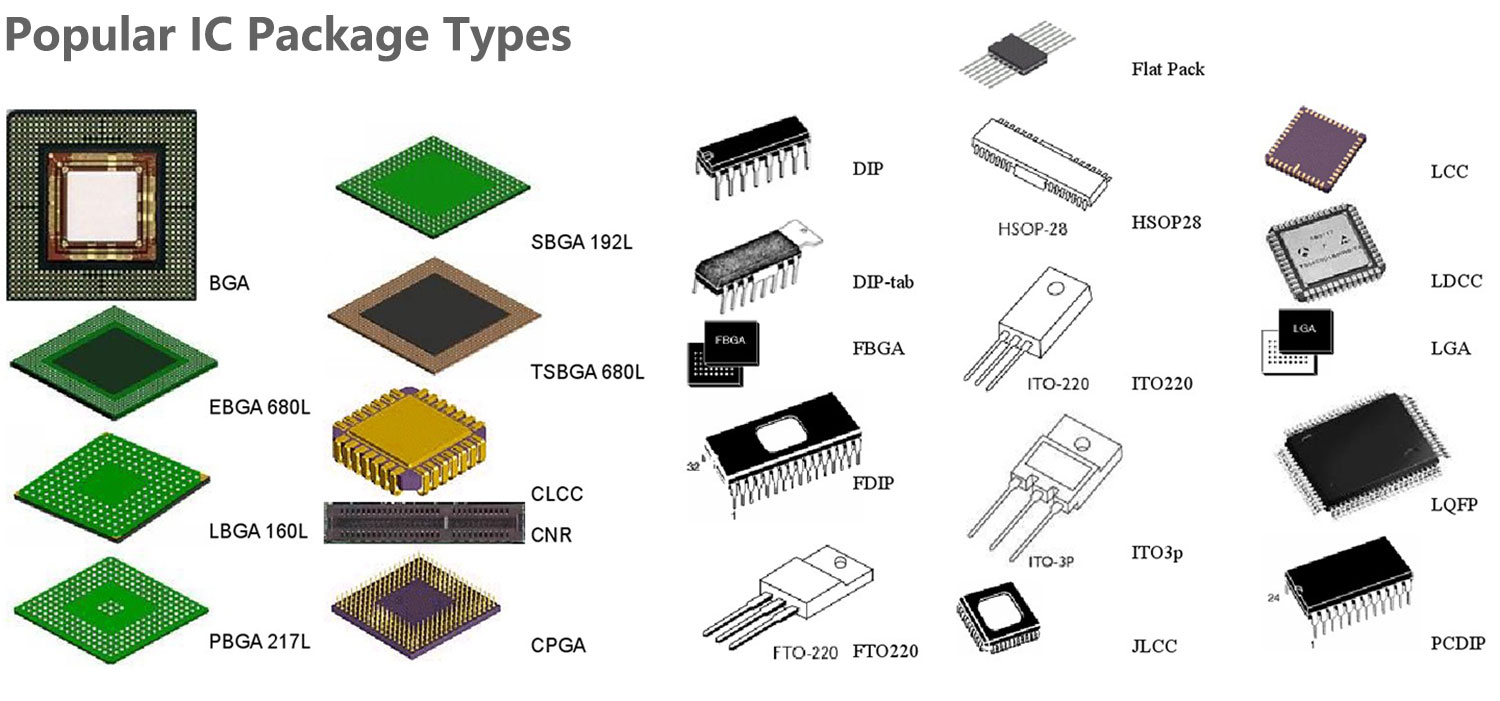
IC substrates are highly diverse. The most practical way to classify them is by the specific packaging architecture they support. Your chosen package dictates the routing density, material, and thermal requirements of the substrate.
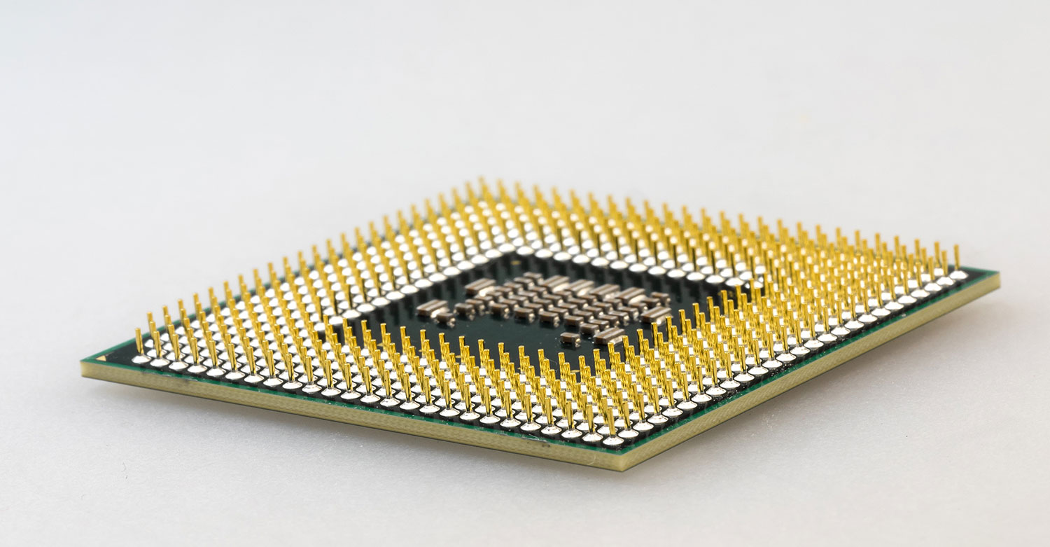
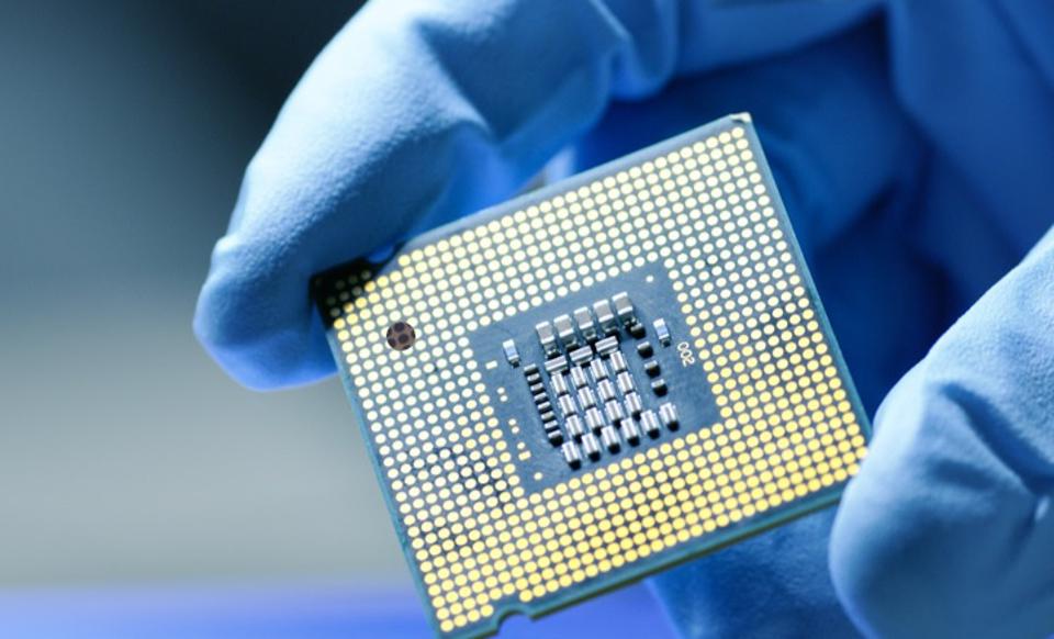
BGA substrates are the workhorses of high-pin-count silicon (typically over 300 pins), such as CPUs, GPUs, and complex FPGAs. Instead of perimeter pins, the bottom of the package features an array of solder balls. BGA substrates must excel at power distribution and heat dissipation, often incorporating dense ground planes and thermal vias.
By definition, a CSP is a package that is no more than 1.2 times the size of the bare silicon die itself. CSP substrates are exceptionally thin and miniaturized, making them the standard choice for mobile devices, memory modules (RAM/NAND), and wearable electronics where real estate is at an absolute premium.
In traditional packaging, the chip faces up. In Flip-Chip packaging, the silicon die is flipped upside down, and its surface pads connect directly to the substrate using tiny solder bumps (micro-bumps). FC substrates (like FCBGA) offer incredibly low signal inductance, minimal circuit loss, and superior thermal dissipation because the back of the die is exposed and can be directly mated to a heat sink. This is the dominant architecture for modern high-performance AI and networking processors.
Choosing the correct dielectric material is the most consequential engineering decision in IC substrate design. The material dictates the Coefficient of Thermal Expansion (CTE), moisture absorption, and signal integrity at high frequencies. With 2026's material shortages, understanding your alternatives is vital.
Pioneered by Mitsubishi Gas Chemical, BT resin is the industry standard for memory, CSP, and RF IC substrates. It boasts a high Glass Transition Temperature (Tg), excellent moisture resistance, and reliable electrical insulation. Its CTE usually ranges between 13 and 17 ppm/°C. While robust, its fiberglass reinforcement limits how fine the laser-drilled microvias can be.
ABF is a thermosetting resin film (without a fiberglass weave) that is laminated onto a core. Because it lacks a woven glass matrix, laser ablation can create exceptionally small, precise microvias, and copper can be patterned at sub-10 µm resolutions. ABF is the undisputed king for high-performance computing (HPC), AI chips, and FCBGAs. The 2026 shortage in ABF precursor materials is a primary driver behind current supply chain bottlenecks.
For extreme environments, power electronics, and aerospace applications, organic resins fall short. Ceramic substrates—typically manufactured from Aluminum Oxide (Al2O3), Aluminum Nitride (AlN), or Silicon Carbide (SiC)—offer unparalleled thermal conductivity and a very low CTE (around 6 to 8 ppm/°C). This CTE closely matches the silicon die (approx. 3 ppm/°C), virtually eliminating thermal mechanical stress during operation.
Used heavily in display drivers and medical implants, flexible IC substrates are formulated from Polyimide (PI) films. They offer excellent dielectric properties and flexibility, making them essential for dynamic applications, though their CTE can swing widely depending on formulation (13 to 27 ppm/°C).
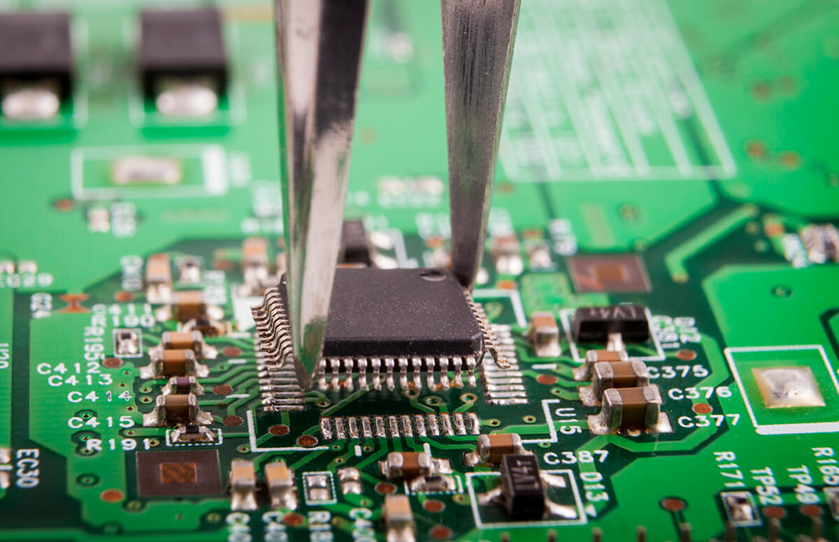
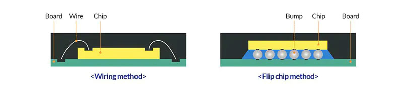
How does the silicon die actually communicate with the IC substrate? There are three primary bonding paradigms in modern packaging:
The oldest and still most widely used technique for lower-cost chips. Automated machines thread microscopic gold, aluminum, or copper wires from the I/O pads on the top of the chip to the corresponding plated pads on the IC substrate. While cost-effective, wire bonds introduce parasitic inductance, making them less suitable for cutting-edge high-frequency RF or AI processing.
As mentioned earlier, Flip Chip bonding relies on an array of solder bumps placed directly on the active surface of the die. The die is flipped, aligned, and reflow-soldered to the substrate. An epoxy "underfill" is then injected between the die and substrate to distribute thermal and mechanical stress. This technology allows for thousands of I/O connections across the entire die area, rather than just the perimeter.
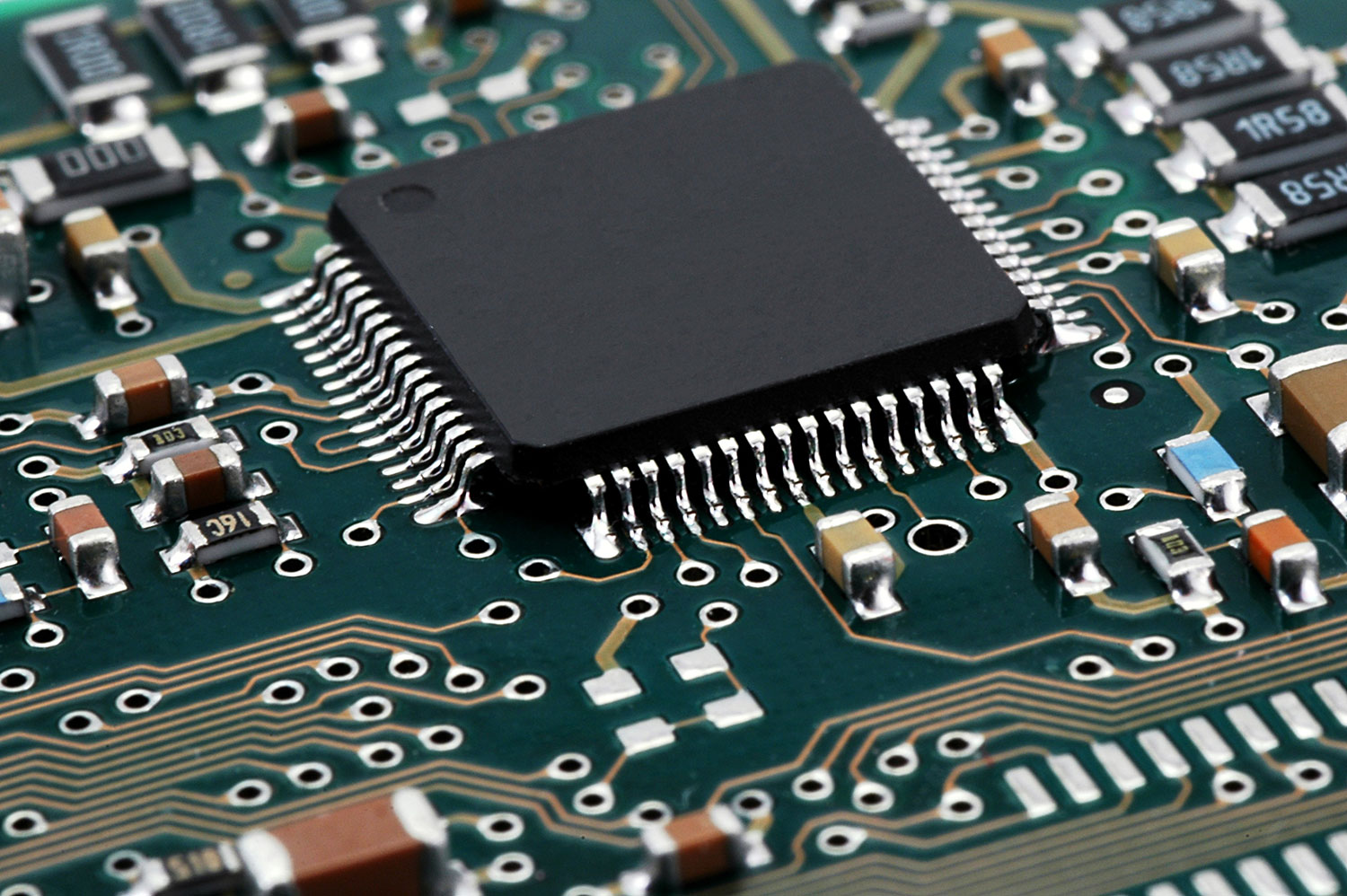
TAB involves bonding a bare integrated circuit directly to a fine-pitch flexible printed circuit (FPC) usually made of polyimide. The chip is thermocompression-bonded to the copper traces on the polymer tape. This is frequently seen in LCD/OLED display drivers and compact consumer electronics.
Producing an IC substrate is closer to semiconductor fabrication than traditional PCB routing. When you order a turnkey PCB or IC carrier, the fabrication facility will utilize one of three primary methodologies depending on your line/space requirements.
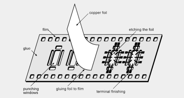
This is the traditional printed circuit board manufacturing method. It starts with a copper-clad laminate. A photoresist dry film is applied, exposed, and developed to protect the desired circuit traces. The unprotected copper is then chemically etched away.
The Engineering Bottleneck: Isotropic (lateral) etching. As the chemical etches downward, it also eats into the sides of the copper traces. Because of this "undercut," SP is generally limited to line widths greater than 50 µm (2 mil). It is suitable for standard boards but insufficient for high-density IC substrates.
To overcome etching limitations, the Additive Process builds the copper traces from the ground up. It begins with a bare insulating substrate coated with a photosensitive catalyst. The circuit pattern is exposed, and copper is deposited via an electroless chemical bath only where the catalyst was activated.
The Engineering Bottleneck: Because no etching is required, AP can achieve extreme precision (sub-20 µm). However, achieving strong adhesion between the electroless copper and the bare resin is notoriously difficult, making this process expensive, slow, and mostly reserved for ultra-niche WB or FC substrates.
MSAP is the undisputed industry standard for manufacturing high-end IC substrates and Substrate-Like PCBs (SLP).
How it works: The process begins with a very thin electroless copper seed layer (typically 1-2 µm) deposited over the dielectric. A thick dry film photoresist is applied and patterned to expose the areas where traces are needed. Copper is then electroplated upward within these trenches. Finally, the photoresist is stripped, and a very quick "flash etch" removes the ultra-thin seed layer between the traces.
Why it wins: Because the final flash etch only has to chew through 1 µm of copper, lateral etching is practically eliminated. MSAP offers high production yields, reliable trace geometries (down to 10/10 µm L/S), and better cost efficiency than pure additive processes.
Designing an IC substrate is only half the battle; ensuring it yields well on the manufacturing floor is what separates successful hardware launches from costly delays. Whether you are dealing with a quick turn PCB prototype or mass PCBA production, engineers must design for manufacturability (DFM).
IC substrates are incredibly thin (often <0.2mm). During the extreme heat of the SMT reflow oven, the silicon die, the copper traces, and the organic resin expand at different rates. This CTE mismatch causes the board to warp like a potato chip, leading to cracked solder bumps or open circuits. Engineers must balance copper distribution across layers (copper thieving) to ensure symmetrical thermal mass. In 2026, manufacturers are heavily relying on low-CTE laminates to mitigate this.
Blind and buried vias in substrates are ablated using precision UV or CO2 lasers. Challenges include ensuring the laser completely cleans the resin residue from the target pad (desmear process) and achieving void-free copper filling during electroplating. A trapped air bubble inside a microvia will eventually expand and cause a failure in the field.
For flip-chip bumping to succeed, the ENIG or ENEPIG surface finish must be perfectly planar. Variation in gold plating thickness across a panel will result in uneven solder joints. Fabricators employ rigorous chemical bath controls and X-ray fluorescence (XRF) testing to measure plating thickness down to the nanometer.
Due to the microscopic scale of substrate traces, traditional electrical testing is insufficient. Modern substrate facilities utilize:


The ubiquity of high-density packaging means IC substrates are embedded in virtually every modern electronic vertical:
Expert Insight: The fundamental difference lies in "micron-level" precision. While standard high-density PCBs typically have line widths and spacing (L/S) above 50 µm, IC substrates (such as those used in FC-BGA) require 5 µm to 20 µm or even less. Furthermore, substrates utilize advanced materials like BT resin or ABF (Ajinomoto Build-up Film). These materials are engineered to closely match the Coefficient of Thermal Expansion (CTE) of silicon chips, preventing solder joint fractures during thermal cycling—a level of stability standard FR4 cannot provide.
Expert Insight: The bottleneck is caused by the monopolistic nature of ABF material supply combined with the low yield rates of high-layer-count FC-BGA processes. With the explosion in demand for AI chips (such as those from NVIDIA), global production capacity has been heavily pre-booked by industry giants. This leaves smaller players struggling with a supply chain that cannot scale quickly enough to meet the surge in high-performance computing requirements.
Expert Insight: This is a major pain point for small-to-medium enterprises. IC substrate production lines are entirely distinct from standard PCB lines, requiring much higher cleanliness classes and specialized Laser Direct Imaging (LDI) equipment. While most substrate manufacturers demand high minimum order quantities (e.g., 10k+ units), some leading quick-turn PCB providers are beginning to offer mSAP (Modified Semi-Additive Process) services to support prototyping at the 20 µm - 30 µm level.
Expert Insight: Unlike the traditional "subtractive process" which relies on etching and often results in "undercutting" or sloped trace edges, mSAP (Modified Semi-Additive Process) involves coating a thin copper seed layer and then electroplating to build up the traces. This results in vertical sidewalls and highly precise geometries, allowing for much tighter line spacing and superior impedance control, which is essential for modern smartphones and wearable electronics.
IC substrates are the unsung heroes of the electronics revolution, forming the vital mechanical and electrical link between bleeding-edge silicon and the rest of the world. As 2026 pushes the boundaries of AI packaging and introduces complex supply chain pricing dynamics, understanding material science (ABF vs. BT), manufacturing processes like MSAP, and stringent DFM rules is non-negotiable for hardware teams.
Navigating these complexities—from strict warpage control to sub-micron surface finish tolerances—requires a reliable and technologically advanced manufacturing partner. Whether you are validating a new BGA design and need a quick turn PCB, or you are scaling up to full-volume PCB assembly, having experts review your Gerber and ODB++ files can save countless weeks and thousands of dollars in scrapped prototypes.
Ready to bring your advanced IC packaging or high-density board to life? At NextPCB, we specialize in high-reliability low cost PCB fabrication and seamless PCBA services. Our engineering team is equipped to guide you through substrate material selection, impedance control, and DFM optimization to ensure maximum yield.
Contact NextPCB today for a comprehensive engineering review and a fast, accurate quote on your next high-performance printed circuit board project.

Still, need help? Contact Us: support@nextpcb.com
Need a PCB or PCBA quote? Quote now

