Flexible PCBs (FPCs), also known as flex PCBs or flexible circuit boards, are printed circuit boards made of bendable substrate materials such as polyimide (PI), allowing them to twist, fold and conform to tight spaces or precise shapes. Flexible printed circuit boards remain indispensible in applications where the space is limited or non-planar, or where dynamic movement is required.
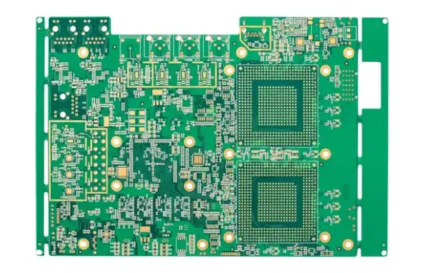
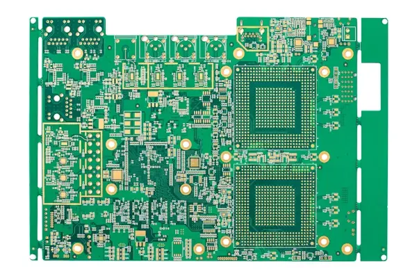
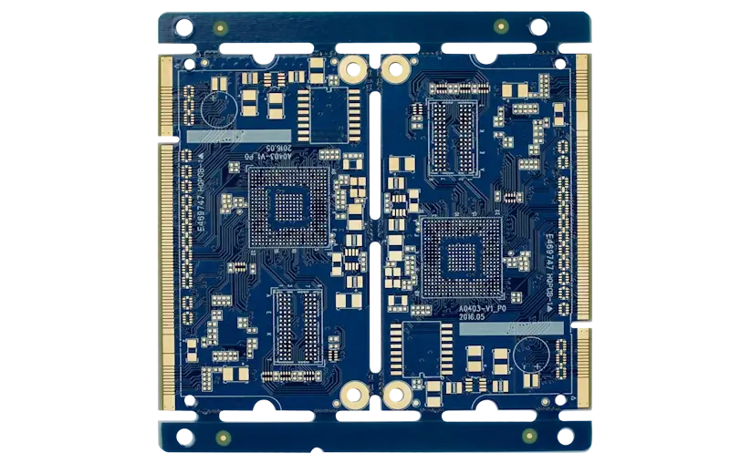
As a flex PCB manufacturer, NextPCB fabricates single, double and multilayer flex circuits up to IPC Class 3 under IATF 16949, ISO 13485 and ISO 9001 certified processes—covering everything from simple flex cables to rigid-flex assemblies. The unique properties and advantages of flex PCBs make them suitable for a wide range of applications which would be impossible or vastly inferior with conventional rigid alternatives.
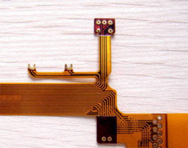
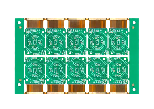
Custom flex cable PCBs with various stiffeners and connectors
NextPCB provides PCB manufacture and assembly of various flex PCB types from simple flex cables to the most demanding applications including:
Single, double and multilayer flex PCBs up to IPC Class 3
Flex PCB assembly
Various stiffener materials and thicknesses
EMI shielding, non-conductive and conductive adhesive backing
Rigid-flex PCB manufacture
What are Flexible PCBs?
Flex PCBs are printed circuit boards constructed entirely of flexible materials. The most common type is made of polyimide (PI) where copper traces and pads are laminated onto a thin sheet of PI, which are then covered with another sheet of PI film called the coverlay. Adhesives hold all the layers together to make a thin printed circuit board that can withstand thousands of bend cycles while maintaining mechanical and electrical performance. For a deeper walkthrough of construction, stack-ups and design rules, see our Ultimate Guide to FPCB.
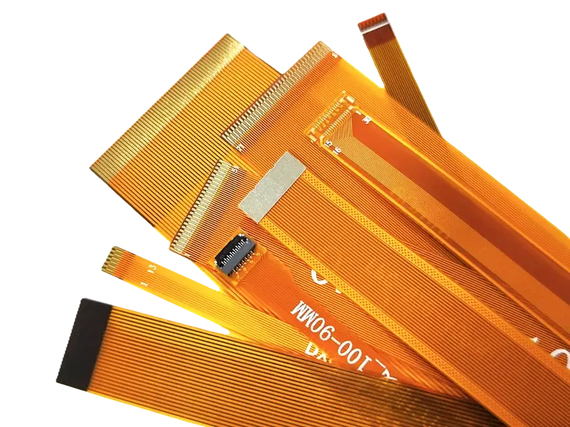
Most FPCs are yellow due to the natural color of polyimide base material. Though they can be dyed different colors.
Types of Flexible Printed Circuit Boards
Flex PCBs come in many different forms and can be manufactured using a variety of different materials and techniques to suit different applications. Here are some of the most common:
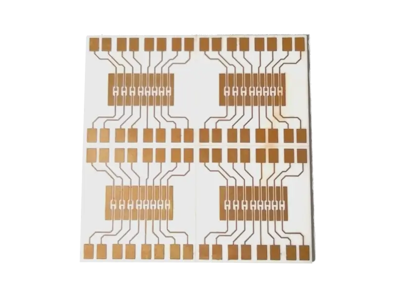
Polyimide Flex PCBs
PI, also known by the branded name, Kapton®, polyimide is a strong temperature resistant polymer found everywhere from solar panels to satellite thermal insulation. It makes a great material for flex PCBs thanks to it's exceptional thermal resistance and electrical insulation properties and can easily integrate multiple conductive layers while maintaining a thin profile.
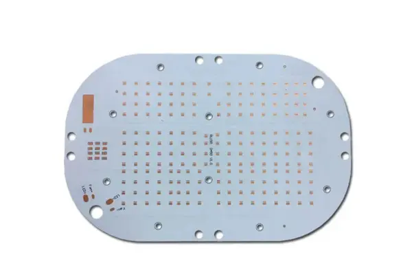
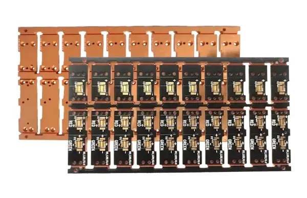
LED Flex PCBs
LED flex PCBs for lighting applications include LED strips, LED lightbulbs and torches. Polyimide is commonly used for the base substrate but the surface is covered in a flexible white or black solder mask to offer better reflective or absorption properties. Thick aluminum foil backing and heavy copper are options to improve heat transfer and reinforce the PCBs.
Thin FR4 Flex PCBs
Circuit boards with a degree of flexibility can be achieved using thin FR4 substrates. While regular FR4 boards have a final thickness of 0.8 to 2.5mm, thicknesses as low as 0.4mm to 0.1mm are possible with thinner cores which give the boards a degree of flex. Though less common than PI PCBs, these PCBs are suitable for static installations where the PCBs are bent and held in place permanently, or low-flex applications that require minor bending while retaining the advantages of rigid PCBs.
Semi-flex PCBs
Semi-flex PCBs are also made of standard FR4 materials but have the thickness partially milled to create a bend area, effectively achieving a rigid-flex structure. This z-axis milling technique can also be used to create bend areas in metal core PCBs such as aluminum core circuit boards. Such boards are not suited for repeated bending however.
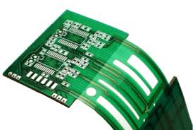
Rigid-Flex PCBs
Rigid-flex circuit boards consist of both rigid and flex areas, typically by sandwiching layers of polyimide between FR4 substrates. The flex sections are reserved for bending and signal transfer while the rigid sections house the components and intricate circuitry, achieving the best of both worlds. Though much more expensive than pure flex PCBs, rigid-flex PCBs offer significant space and weight savings over separate rigid boards joined by connectors. If your project needs a flex rigid PCB manufacturer that also handles assembly, see our Complete Guide to Rigid-Flex PCB Assembly.
Applications and Advantages of Flex PCBs
Flex PCBs offer three primary advantages over their rigid counterparts that make them invaluable in a wide range of products and applications. Their lightweight design, ultra-thin profile and the ability to bend or conform to various configurations mean they can be found in everything from earpods, touch interfaces, foldable electronics, medical devices, mechatronics, light strips, and anything that has an LED or LCD display.
When to consider flex PCBs over rigid PCBs:
When repeated movement & bending is required. Flex PCBs (especially polyimide-based ones) endure thousands of bending cycles without mechanical failure or signal degradation, making them ideal for dynamic applications.
When the electronics needs to conform to irregular shapes. Unlike rigid boards, flex circuits can wrap around non-planar surfaces. For example, wearables need to wrap around the users' body shape for comfort, LEDs in LED bulbs wrap around a curved surface to spread out light equally.
For portable, sleek and lightweight electronics. Flex PCBs, particularly PI flex PCBs, offer unbeatable lightweightedness and ultra-thin profiles, enabling sleek, portable electronics.
When to consider flex cable PCBs over cables and harnesses:
When a cable or harnesses would take too much space. Flex cable PCBs can perform signal transfer reliably while taking up a fraction of the space of cables and harnesses. Their almost negligible thickness and ability to fold over themselves can vastly reduce the volume of end products. Flex board connectors can also be much more discrete and take up less board space than cable connectors.
When the movement of cables needs to be limited. Unlike cables, flex PCBs move freely in two axes rather than three, allowing for some control of it's movement. The design of gantry style flex PCBs are an example exploiting this feature, allowing controlled movement in 3 axis while preventing the PCB getting tangled up or rubbing against objects. Flex PCBs can also help with alignment, take for example interfaces with tactile buttons, the layout of the buttons is fixed by the flex PCB's design.
Limitations of Flex PCBs
While flex PCBs offer a unique set of advantages, their inherent flexibility introduces complexities across the entire product lifecycle, from design to manufacture to assembly and deployment. Engineers should be well aware of the limitations and constraints before beginning a flex PCB design for optimal manufacturability and reliability.
Restricted component placement: Component placement is limited to non-bend areas, areas with low bend frequency or low bend radius. FPCs are flexible, but solder joints are not. Excessive bending can cause joints to crack or tear from the substrate. Stiffeners can be used for reinforcement, however, this takes up space on one side and essentially limits component placement to a single side.
Low component density: Manufacturing limits and tolerances for flexible PCBs are not as refined compared to rigid based alternatives. Alongside the additional bend and mechanical considerations, this impacts how close components and traces can be placed together.
Copper and layer count limitations: The number, thickness and layout of copper layers can have a significant impact on the bend radius and bend frequency. As such, this limits the complexity and current carrying capacity of flex circuits. Design techniques such as using hatched over filled copper pour, removing coverlay in bend areas and using lower copper thicknesses can be used to increase flexiblility in bend areas.
Design challenges: The dynamic and fragile nature of flex PCBs mean extra care and additional design techniques are required to maintain the structural integrity of a flex PCB during it’s lifetime. For more design techniques with examples, take a look at our flex PCB design guide on Wevolver.
Difficulty of manufacture and PCB assembly: While polyimide has excellent heat resistant properties (typically 250-280°C), without careful consideration and process control, flex PCBs are prone to shrinking and delamination during the soldering process. The design of solder fixtures must take this into account and limit exposure to heat to only where necessary. Even for small batch and prototype runs, a fixture is recommended to facilitate component placement and soldering, adding to production costs.
How to Choose a Flex PCB Manufacturer: Capability, Certification & Sampling Process
Not every flex PCB fab can hold tight tolerances across thousands of bend cycles, so vetting a flex PCB manufacturer before you commit a design is worth the extra week of diligence. Below is the checklist NextPCB recommends when comparing flex PCB suppliers for a new program.
Manufacturing Capability Checklist for Flex PCB Fabrication
When comparing flexible printed circuit manufacturers, ask for documented, not marketed, capability data on the following:
Layer count and stack-up flexibility: can the flex PCB manufacturing line handle single, double and multilayer builds, and does it support hybrid rigid-flex stack-ups if your design may migrate there later?
Minimum trace/space and drill diameter: finer geometries (e.g. 2/2 mil trace/space, sub-0.15mm drills) indicate a more mature flex PCB fabrication process, important for dense flex cables and connectors.
Base material sourcing: reputable flex PCB suppliers name their PI laminate brands (e.g. ITEQ, Grace, Doosan, Taiflex) rather than using unbranded stock, since adhesive/adhesiveless RA or ED laminate choice directly affects flex-life.
Coverlay and solder mask options: confirm the flexible pcb manufacturer can offer both PI coverlay and flexible solder mask, plus the colors your design or branding requires.
Stiffener and reinforcement support: FR4, PI, aluminum or stainless steel stiffener options signal a supplier experienced with connector interfaces and mechanical loading.
In-house assembly capability: a flex rigid pcb manufacturer that also runs PCB assembly under the same roof reduces handoff risk between fabrication and SMT, especially for fragile flex boards.
Certifications to Look for in a Flex PCB Supplier
Certifications are the fastest proxy for process discipline at a flex pcb manufacturer, particularly for regulated end markets:
IPC Class 2/3: confirms the fabricator's flex PCB manufacturing meets defined workmanship and reliability standards; Class 3 is typically required for aerospace, medical and other high-reliability designs.
IATF 16949: the automotive quality management standard, relevant if your flex or rigid-flex PCB will go into a vehicle program.
ISO 13485: indicates the supplier's quality system is suited to medical device production, important for implantable or wearable flex circuits.
ISO 9001: baseline quality management certification any serious flex pcb fab should hold.
UL and RoHS compliance: confirms materials and flammability ratings meet safety and environmental regulations for your target markets.
NextPCB's flex and rigid-flex manufacturing lines operate under IATF 16949, ISO 13485, ISO 9001, UL and RoHS-compliant processes, up to IPC Class 3.
Flex PCB Sampling and Prototyping Process
A dependable flex pcb supplier should walk every new design through a structured sampling process before committing to volume tooling:
DFM/Gerber review: the fab checks bend radius, coverlay openings, copper pour hatching and stack-up symmetry against manufacturable limits before quoting.
Material and stack-up confirmation: PI base material, copper weight, adhesive type and stiffener placement are locked in writing.
Prototype fabrication: a small-batch flex PCB fabrication run is built, typically using a soldering fixture to protect the flex substrate during assembly.
Electrical and mechanical verification: AOI, electrical testing and, where specified, bend-cycle or flex-life testing confirm the sample meets spec.
Sample review and iteration: engineering feedback is incorporated before release to volume flexible pcb manufacturing.
For rigid-flex designs specifically, our Rigid-Flex PCB Assembly Guide walks through how this sampling process extends into SMT assembly.
NextPCB Flex PCB Manufacturing Capabilities
At NextPCB, we specialize in a wide variety of flex PCBs, offering a broad selection of options and features for any application, backed by the certifications and process controls outlined above.
Feature
Specification
Flex Circuit Layers
1 to 6 layers
PI Base Material
Brands: ITEQ, Grace, Doosan, Allstar, Thinflex and Taiflex
Adhesive/adhesiveless RA or ED laminates
Covering Type
PI Coverlay or Flexible Solder mask
Surface Finishes
ENIG, OSP and electroplated gold
ENIG Gold Thickness
1 to 3μ"
Flex PCB Thickness
0.1 to 0.45mm
Copper Thickness
1/3 to 2 oz
Min. Trace width/spacing
2/2 mil
Min. Drill Hole Diameter
0.1mm
PCB Solder Mask Color
Coverlay: Yellow, white, black and clear
Solder Mask: Green, red, yellow, orange, black, silver and clear
Compare documented capability data (layer count, trace/space, materials), certifications (IPC Class, IATF 16949, ISO 13485, ISO 9001), and whether the supplier offers in-house assembly and a structured sampling process, not just quoted price.
What certifications should a flex PCB supplier have?
At minimum, look for ISO 9001 and IPC Class 2 or 3 workmanship compliance. For automotive programs, require IATF 16949; for medical or implantable devices, require ISO 13485; for regulated markets, confirm UL and RoHS compliance.
What is the difference between a flex PCB manufacturer and a flex PCB assembler?
A flex PCB manufacturer fabricates the bare flexible circuit (copper on polyimide with coverlay); an assembler populates that circuit with components via SMT/THT. Many flex pcb suppliers, including NextPCB, offer both under one roof to reduce handoff risk.
Can the same supplier handle both flex and rigid-flex PCB manufacturing?
Yes—a flex rigid pcb manufacturer with both flex and rigid-flex lines can carry a design from pure flex cable through a hybrid rigid-flex assembly without re-qualifying a new vendor. See our Rigid-Flex PCB Assembly Guide for process detail.
What happens during flex PCB sampling before volume production?
The fab reviews the design for manufacturability, confirms materials and stack-up, builds a small prototype batch (typically using a soldering fixture), runs electrical/mechanical verification, and incorporates feedback before releasing to full flexible pcb manufacturing.
Browse Different PCB Solutions for Every Need
Looking for the right PCB solution? Explore various types of PCBs to find the perfect match for your project.

 NextPCB Capabilities
 PCB Assembly
 Layer Buildup
 SMD-Stencils
 PCB Design-Aid & Layout
 Mechanics
 Surface
 Quality
 Drills & Throughplating
 Factory & Certificate