- Table of Contents
- What is an LED PCB?
- Key Components
- Classifications of LED PCB
- The Industry Application of LED PCB
- Advantages and Disadvantages of LED PCBs
- Optimizing Your Design: Key Considerations for High-Performance LED PCBs
- PCB LED Assembly Methods: Through-Hole vs. SMD
What is an LED PCB?
Light-emitting diodes (LEDs) have revolutionized the landscape of lighting technology. They offer superior energy efficiency, extended lifespan, and design flexibility compared to traditional incandescent bulbs. However, to harness the power of LEDs in various applications, a crucial component comes into play: the LED PCB, or Printed Circuit Board.
An LED PCB is a specialized circuit board specifically designed for mounting and powering Light Emitting Diodes. It functions as the foundation upon which LEDs are soldered, providing not only electrical connections but also physical support. Imagine it as a roadmap with designated pathways for electricity to flow and illuminate the LEDs.
Key Components
Here's a breakdown of its key components:
- Substrate: This forms the base of the PCB and is typically made from a non-conductive material like FR-4 (a flame-retardant epoxy laminate). In some high-power applications, aluminum PCBs with superior heat dissipation properties are used.
- Copper Traces: These are thin, metallic pathways etched onto the substrate that act as electrical conductors, carrying current to the LEDs.
- Solder Pads: These are designated areas on the copper traces where the LEDs are soldered for electrical connection.
- Resist: This is a protective layer applied to the substrate, leaving only the desired copper traces exposed.
- Components: Additional components like resistors, capacitors, and voltage regulators might be present depending on the LED circuit's design.
Classifications of LED PCB
There are several ways to categorize LED PCBs, but two prominent classifications are based on material and application:
Material:
- Standard FR-4 PCBs: These are the most common type, offering a cost-effective solution for low to medium power applications.
- Metal Core PCBs: Primarily made of aluminum, these PCBs excel at heat dissipation, making them ideal for high-power LED applications.
Application:
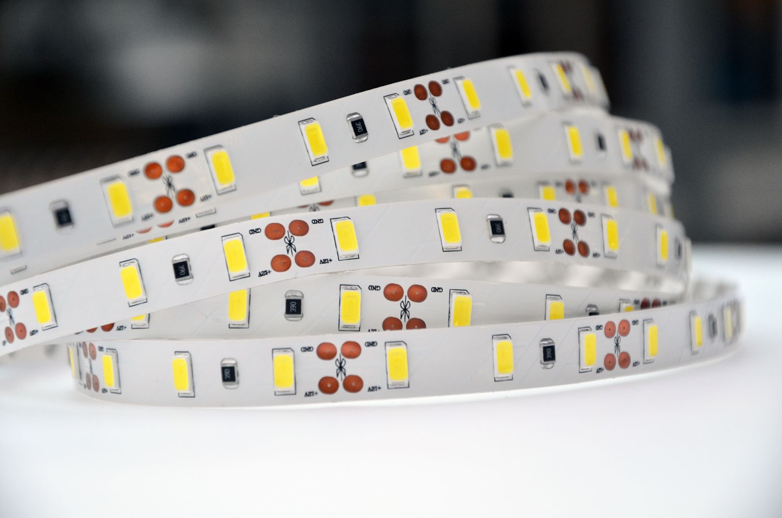
- LED Strip PCBs: These linear PCBs hold multiple LEDs in a flexible or rigid strip format, commonly used in decorative lighting and backlighting applications.
- LED Panel PCBs: These PCBs hold a matrix of LEDs to create larger light panels, often used in commercial and industrial lighting.
- High Brightness LED (HB LED) PCBs: Designed for applications requiring intense light output, such as automotive headlights and architectural lighting.
- Backlight Unit (BLU) PCBs: These PCBs illuminate displays in electronic devices like TVs and smartphones.
The Industry Application of LED PCB
LED PCBs, with their unique blend of functionality and design flexibility, have infiltrated a vast array of applications, transforming the way we illuminate our world.
General Lighting:
LED PCBs are at the heart of the LED lighting revolution, replacing traditional incandescent and fluorescent bulbs in homes, offices, and commercial spaces. Their energy efficiency translates to significant cost savings and reduced environmental impact. Additionally, the ability to control color temperature and dimming capabilities opens doors for creating dynamic and personalized lighting experiences.
Consumer Electronics:
From the vibrant displays of smartphones and tablets to the backlighting of keyboards and laptops, LED PCBs are ubiquitous in consumer electronics. Their compact size and design flexibility allow for seamless integration within these devices, enabling features like high-resolution displays and power-efficient operation.
Automotive Lighting:
LED headlights, taillights, and brake lights are rapidly becoming the standard in the automotive industry. LED PCBs offer superior brightness, faster response times, and lower energy consumption compared to traditional halogen bulbs. This translates to improved safety, reduced fuel consumption, and a distinctive aesthetic for modern vehicles.
Architectural Lighting:
Architects and designers leverage LED PCBs to create stunning and energy-efficient lighting solutions for buildings and landscapes. The ability to control color precisely and integrate LEDs into various forms allows for creative illumination of facades, monuments, and interior spaces.
Medical Devices:
LED PCBs find applications in specialized medical equipment, providing precise and controllable illumination for surgical procedures, diagnostic instruments, and medical displays. Their compact size and heat dissipation capabilities make them ideal for these sensitive applications.
Display Technology:
Large format displays, video walls, and digital signage all rely on LED PCBs to deliver high-resolution visuals. The ability to customize LED density and color temperature allows for creating captivating displays for advertising, entertainment, and information dissemination.
Advantages and Disadvantages of LED PCBs
Advantages:
- Improved Efficiency: LEDs themselves are highly efficient at converting electricity into light, and the PCB design can further optimize this process by minimizing power loss through heat dissipation.
- Compact Design: PCBs can be designed in various shapes and sizes to fit diverse applications, enabling the creation of compact and lightweight lighting solutions.
- Design Flexibility: The ability to customize the PCB layout allows for intricate lighting patterns and unique configurations.
- Durability: PCBs are generally robust and resistant to shock and vibration, making them suitable for demanding environments.
- Scalability: LED PCBs can be easily scaled up or down to accommodate various lighting needs.
Disadvantages:
- Heat Management: High-power LED applications require careful PCB design and appropriate materials to manage heat effectively. Overheating can shorten the lifespan of LEDs.
- Manufacturing Complexity: Multilayer PCBs with complex circuitry can be expensive to manufacture compared to simpler designs.
- Repair Challenges: Depending on the complexity of the PCB, individual LED repair might not be feasible, requiring replacement of the entire board.
Optimizing Your Design: Key Considerations for High-Performance LED PCBs
To navigate these challenges and create an LED PCB that maximizes LED performance and system efficiency, several factors need careful consideration:
Thermal Management:
Perhaps the most critical aspect of LED PCB design is thermal management. Here are some effective strategies:
- Multi-layer PCBs with Thermal Vias: Utilize PCBs with multiple copper layers for improved heat distribution. Embedding thermal vias – tiny holes filled with heat-conductive material – connects these layers, creating a more efficient heat transfer path from the LEDs to the external environment.
- Copper Plane Heat Dissipation: Maximize the use of large copper planes on the PCB. These planes act as heat spreaders, drawing heat away from the LEDs and radiating it outwards.
- External Heat Sink Integration: For situations where internal heat dissipation isn't sufficient, consider incorporating external heat sinks. These metal components are designed to absorb and dissipate large amounts of heat, ensuring optimal thermal performance.
Power Delivery and Driver Circuitry:
Precise control over the current and voltage supplied to the LEDs is essential for their longevity and color consistency. Here's what to consider:
- Driver Circuit Design: The driver circuit regulates the power delivered to the LEDs. A well-designed driver circuit ensures the LEDs receive the correct current for optimal brightness while minimizing power consumption. Techniques like pulse width modulation (PWM) can be employed for further efficiency gains.
- Component Selection: Choose high-quality components for the driver circuit, including efficient voltage regulators and low-resistance inductors. These components minimize power losses within the circuit itself.
Electromagnetic Interference (EMI) and Noise Control:
EMI can disrupt the operation of nearby electronics and cause unwanted flickering in the LEDs. Here's how to mitigate EMI:
- Grounding Techniques: Implement a well-defined grounding scheme to provide a low-impedance path for EMI currents. This helps prevent them from radiating and interfering with other circuits.
- Component Selection: Select components with lower EMI emissions, such as shielded inductors and capacitors with internal dampening mechanisms.
- Layout Strategies: Employ proper layout techniques to minimize EMI. This includes minimizing loop areas in the PCB traces, keeping high-current and high-speed signals separated, and using proper shielding techniques.
Material Selection:
The choice of PCB material significantly impacts thermal performance. Here's why material selection matters:
- High-Thermal Conductivity Materials: Utilize PCBs fabricated with materials like aluminum or metal core. These materials offer superior thermal conductivity compared to traditional FR4, effectively drawing heat away from the LEDs.
- Flexible and Rigid-Flex LED PCBs: Traditional rigid PCBs may not be suitable for all applications. For situations requiring unique form factors or space constraints, flexible and rigid-flex PCBs offer a compelling solution. These PCBs incorporate flexible sections that can bend and twist, allowing for innovative lighting designs in curved surfaces or tight spaces.
Integrated Circuit (IC) Technology Integration:
Advancements in miniaturization have opened doors for embedding IC technology directly within the PCB itself. This eliminates the need for separate driver boards, leading to a more compact and efficient design. Additionally, integrating driver ICs directly onto the PCB allows for closer proximity to the LEDs, potentially improving performance and reducing EMI.
Layout and Routing:
Careful planning of the PCB layout is crucial for both electrical performance and thermal management. Here are some key considerations:
- Trace Width Optimization: Optimize the width of the copper traces to minimize resistance and ensure adequate current carrying capacity.
- Minimizing Loop Inductance: Pay close attention to minimizing loop inductance in the power delivery paths. Loop inductance can cause voltage spikes and EMI issues. Techniques like keeping traces short and wide, and employing proper component placement, can help achieve this.
- Proper Component Placement: Strategically place LEDs and other heat-generating components to ensure efficient thermal transfer. This may involve grouping LEDs together to leverage the heat sink effect or positioning them near areas with good heat dissipation potential.
PCB LED Assembly Methods: Through-Hole vs. SMD
There are two primary methods for attaching LEDs to a PCB:
Through-Hole Assembly:
This traditional method utilizes LEDs with long leads designed to be inserted through pre-drilled holes in the PCB. The leads are then soldered to the corresponding pads on the opposite side of the board.
SMD (Surface-Mount Device) Assembly:
This method employs LEDs with tiny terminals or contacts directly on their surface. These LEDs are placed directly onto designated solder paste deposits on the PCB and then soldered using a reflow oven.
Advantages of SMD Assembly over Through-Hole Assembly for LEDs:
- Miniaturization: SMD LEDs are significantly smaller than through-hole LEDs, enabling a much smaller footprint on the PCB. This allows for the creation of compact and lightweight devices, ideal for space-constrained applications like smartphones and wearables.
- Enhanced Design Flexibility: The compact size of SMD LEDs opens doors for intricate and high-density LED circuit designs. Designers can place LEDs closer together, enabling complex lighting patterns and innovative lighting solutions.
- Improved Performance: SMD LEDs often offer lower thermal resistance compared to through-hole LEDs. This allows for better heat dissipation, leading to improved reliability and potentially higher light output.
- Faster and More Cost-Effective Assembly: SMD components are ideally suited for high-speed, automated assembly processes using Surface Mount Technology (SMT). This translates to faster production times and lower labor costs compared to manual placement of through-hole components.
Through-hole assembly might still be preferable in some scenarios:
- Lower upfront costs: For small-scale projects or prototyping, through-hole components can be easier and cheaper to work with due to the lack of specialized equipment required for SMT.
- Easier hand soldering: Through-hole LEDs can be easily soldered by hand using basic soldering tools, making them a good choice for hobbyists and DIY projects.
- Stronger mechanical connection: The through-hole method provides a more robust mechanical connection between the LED and the PCB, which might be advantageous for applications with high vibration or shock.
Conclusion
LED PCBs have become an integral part of modern lighting and electronics, offering unparalleled efficiency, design flexibility, and longevity. With the right materials, proper thermal management, and careful assembly methods, LED PCBs can maximize performance across a wide range of applications, from consumer electronics to automotive lighting.
>> Recommeng reading: Ceramic PCB vs FR4 vs Metal-Core: Substrates for Thermal Management
Ready to Build Your LED PCB?
If you're considering creating or optimizing your own LED PCB, we’re here to help! Whether you're working on a small-scale project or a large commercial application, expert guidance can make all the difference. Contact us today to get started on your custom LED PCB design and ensure your project shines bright!
About the Author
With extensive experience in the PCB and PCBA industry, Stacy has established herself as a professional and dedicated Key Account Manager with an outstanding reputation. She excels at deeply understanding client needs, delivering effective and high-quality communication. Renowned for her meticulousness and reliability, Stacy is skilled at resolving client issues and fully supporting their business objectives.

 Surface


 NextPCB Capabilities
 PCB Assembly
 Layer Buildup
 SMD-Stencils
 PCB Design-Aid & Layout
 Mechanics
 Quality
 Drills & Throughplating
 Factory & Certificate
 PCB Assembly Factory Show
Certificate
PCB Assembly Factory Show
Certificate


