NextPCB Highlights Advanced PCB Technologies at electronica 2026
Posted: 04:58 PM November 13, 2026writer: Viviane
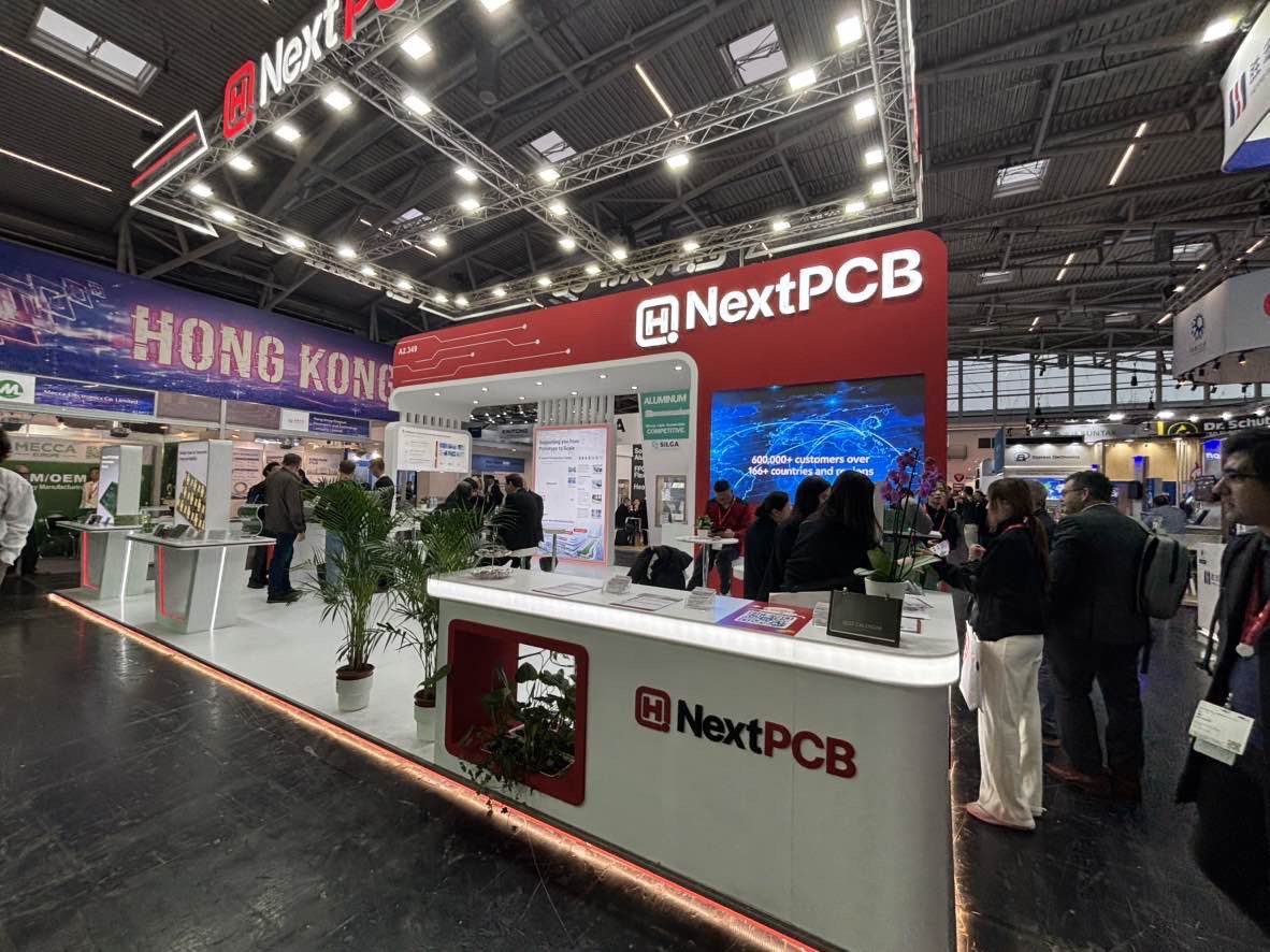
NextPCB, a one-stop PCB and PCBA manufacturing solutions provider, has successfully concluded its four-day exhibition at electronica 2026, held November 10–13 at Messe München, Germany. At Booth A2-349, NextPCB showcased its advanced PCB manufacturing technologies, connected with engineers and industry partners from more than 20 countries and regions, and demonstrated its capabilities in complex PCB fabrication through a dedicated microsection sample gallery.
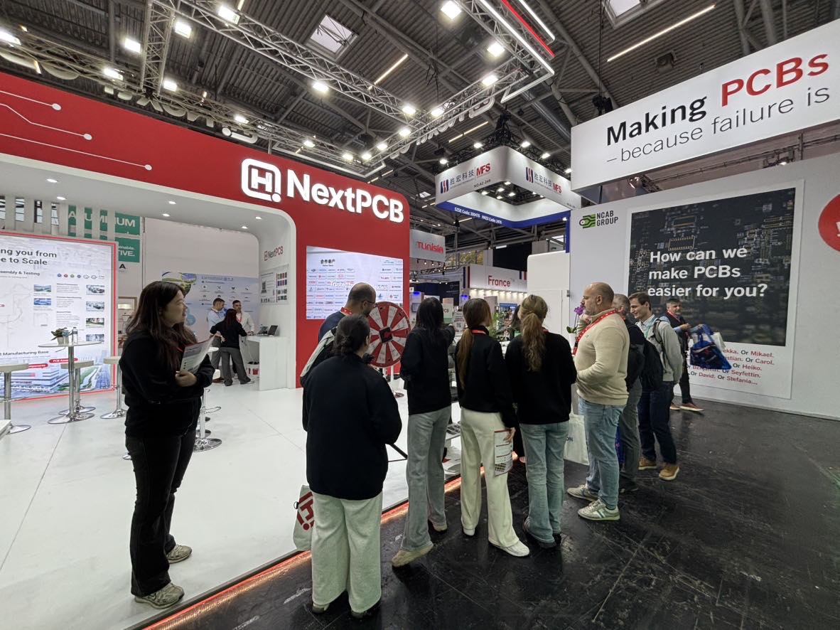
NextPCB welcomed visitors at Booth A2-349 during electronica 2026 in Munich.
Advanced PCB Manufacturing Solutions for Next-Generation Industries
At electronica 2026, NextPCB highlighted its comprehensive manufacturing capabilities, presenting PCB solutions designed to meet the increasingly demanding requirements of modern electronics applications.
High-Speed & Advanced Multilayer PCBs
Supporting up to 40 layers, HDI III structures, and 2.5/2.5 mil line width and spacing, NextPCB provides advanced multilayer PCB solutions using high-performance laminates from leading material suppliers, including Rogers, Isola, and TUC. Combined with backdrilling and controlled impedance technologies, these capabilities support demanding applications in telecommunications, IoT, security, and medical electronics.
Power & Automotive PCB Solutions
With heavy copper capabilities of up to 10 oz, Metal Core PCBs, and embedded copper coin technologies, NextPCB supports high-current and thermal management requirements across automotive electronics, industrial automation, and energy applications. Its manufacturing capabilities also support demanding quality requirements, including IPC Class 3 applications.
Flexible & Rigid-Flex PCBs
NextPCB also presented its 1–6 layer flexible PCB solutions, designed to support compact, lightweight, and space-efficient electronic products, including consumer electronics and wearable devices.
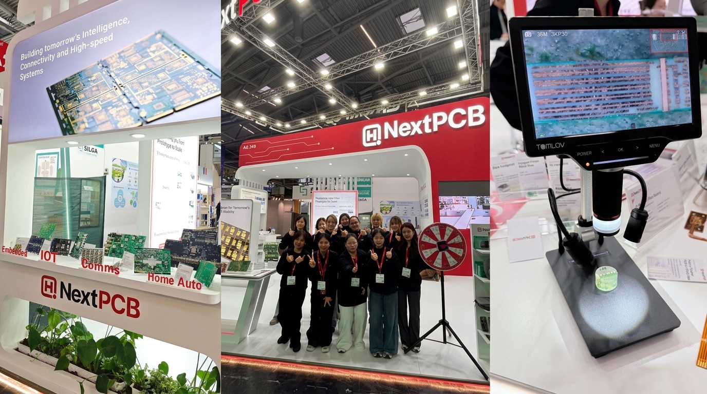
One of the standout attractions at Booth A2-349 was NextPCB's dedicated Microsection Sample Gallery, featuring 19 distinct PCB cross-sectional samples that allowed visitors to examine complex internal PCB structures up close.
The collection showcased a variety of advanced manufacturing structures and processes, including HDI 3 stacked vias, copper-filled blind vias, epoxy-filled and capped vias, embedded copper coins, and heavy copper structures.
By presenting these samples in a tangible, easy-to-examine format, NextPCB demonstrated its manufacturing expertise in precision copper plating, dielectric thickness control, via filling, and complex multilayer PCB fabrication. The display also provided engineers with a practical opportunity to explore how advanced PCB structures translate into real-world manufacturing capabilities and product reliability.
Visitors could explore NextPCB's displays and examine PCB structures through close-up inspection.
Industry Insights from Renowned Hardware Design Educators
NextPCB's presence at electronica 2026 was further enriched by special appearances from renowned hardware design educators and industry voices, including Robert Feranec, Founder of FEDEVEL Academy, and Petr Dvořák.
Throughout the exhibition, they engaged with visiting engineers and hardware developers, exchanging practical PCB design insights and discussing emerging challenges in modern hardware development. Their participation brought additional technical depth to the booth experience and reinforced NextPCB's connection with the global hardware engineering community.
Connecting with the Global Hardware Community
Beyond technical demonstrations and engineering consultations, NextPCB created an engaging booth experience through interactive activities, prize giveaways, and face-to-face conversations with visitors.
The four-day exhibition provided valuable opportunities for the NextPCB team to connect with engineers, hardware developers, procurement professionals, and potential business partners from around the world. These conversations offered insights into evolving market demands and the manufacturing challenges faced by electronics companies across different industries.
Visitors connect with the NextPCB team at Booth A2-349.
“electronica 2026 gave us a valuable opportunity to meet engineers and hardware innovators from around the world. We had meaningful conversations about the challenges of modern PCB design and manufacturing. At NextPCB, we're committed to helping customers turn complex designs into reliable products, from initial prototypes to production.”
— Ivy Li, Head of International Business at NextPCB
From Prototype to Production with NextPCB
Although electronica 2026 has come to a close, NextPCB remains committed to supporting engineers, hardware developers, and electronics companies worldwide.
From PCB prototyping and PCBA assembly to advanced manufacturing and volume production, NextPCB provides integrated manufacturing solutions to help customers bring their electronic designs to life.


 NextPCB Capabilities
 Process Capabilities
 PCB Design-Aid & Layout
 Quality
 Drills & Throughplating
 Factory & Certificate
 PCB Assembly Factory Show
Certificate
 NextPCB Capabilities
 PCB Assembly
 Process Capabilities
 PCB Design-Aid & Layout
 Quality
 Drills & Throughplating
 Factory & Certificate



 Quote now