
 Surface


Stacy Lu

 NextPCB Capabilities
Printed Circuit Boards
NextPCB Capabilities
Printed Circuit Boards
 PCB Assembly
 Layer Buildup
 SMD-Stencils
 PCB Design-Aid & Layout
 Mechanics
 Quality
 Drills & Throughplating
 Factory & Certificate
 PCB Assembly Factory Show
Certificate
PCB Assembly Factory Show
Certificate
Support Team
Feedback:
support@nextpcb.com


Introduction
As the demand for 5G communications, wearable technology, and high-performance computing accelerates, PCB design is being pushed to its physical limits: lighter, thinner, shorter, and smaller. High-Density Interconnect (HDI) technology has become the core enabler for achieving these goals.
However, an HDI PCB is defined by more than just finer traces. Its foundation lies in the Stackup Design. A well-engineered stackup not only determines manufacturability and cost but also plays a pivotal role in Signal Integrity (SI) and Power Integrity (PI).
This article analyzes common HDI stackup types—such as 1+N+1 and 2+N+2—based on the latest IPC-2226 standards, helping you make informed decisions for your next complex design project.
Table of Contents
HDI stackups rely primarily on Microvias to achieve interlayer connectivity. Unlike traditional through-hole boards, HDI utilizes laser drilling technology to create minute blind and buried vias, significantly increasing routing density.
In industry terminology, the formula i + N + i is commonly used to describe HDI structures:
For a comprehensive understanding of HDI definitions and benefits, please refer to our detailed guide: What is HDI PCB?
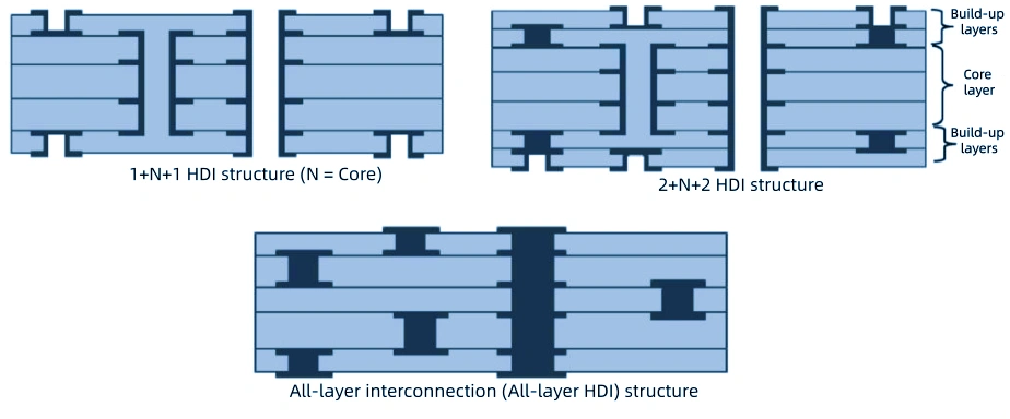
The IPC-2226 standard categorizes HDI products into six primary types (Type I through Type VI). In practical engineering applications, Type I, Type II, and Type III are the most prevalent, corresponding to what is commonly known as single-build (1-step), double-build (2-step), and multi-build HDI.
Structure Description:
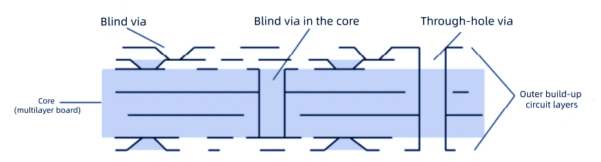
This is the entry-level form of HDI. It consists of a central laminated core with one build-up layer laminated on both the top and bottom.
Typical Type I (1+N+1) HDI PCB stackup illustrating blind vias between the outer layers and the laminated core, commonly used for mid-density BGA fan-out designs.
>> Recommend reading: HDI PCB Design Guidelines for BGA Fanout & Stackup Planning
Advantages:
Applications:
Mid-range smartphone motherboards, handheld GPS devices, and basic control modules.
Structure Description:
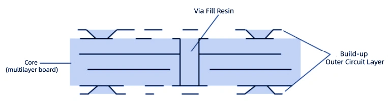
The primary distinction between Type II and Type I lies in the treatment of the Core. Type II allows for Buried Vias within the core. These vias are typically filled with resin and plated over (Via-in-Pad process), allowing the surface blind vias to land directly on the buried via pads (if process capabilities permit) or to be staggered.
Type II HDI PCB structure featuring buried vias inside the core, enabling higher routing density and improved power and ground plane continuity.
Key Features:
Structure Description:
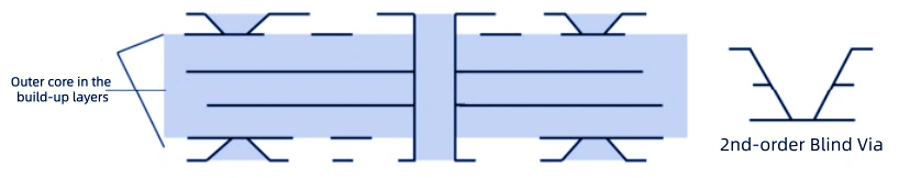
When design density increases to a point where a single build-up layer is insufficient, Type III structures are employed. This involves laminating build-up layers twice on both sides of the core.
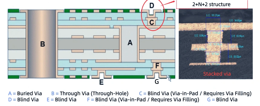
2+N+2 HDI PCB stackup with double build-up layers on both sides of the core, supporting multi-tier microvias for high-density interconnect routing.
Staggered microvia configuration in a Type III HDI PCB, offering improved manufacturability and reliability compared to fully stacked vias.
Advantages:
Applications:
High-end 5G smartphones, AI acceleration cards, DDR4/DDR5 memory modules, and medical devices with strict size constraints.
As technology evolves, the traditional distinction between "Core" and "Build-up" has blurred in ultra-high-end applications, evolving into ELIC (Every Layer Interconnect). In this structure, the board lacks traditional mechanical through-holes; all interlayer connections are achieved via stacked laser microvias, allowing for interconnections between any two layers.
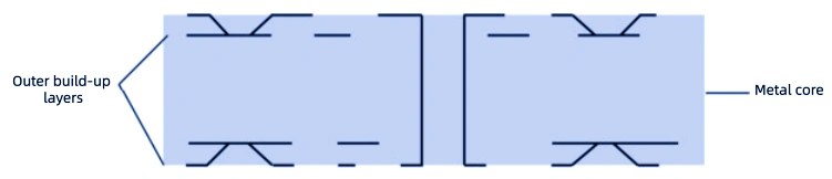
ELIC (Every Layer Interconnect) PCB structure where all layers are interconnected using stacked laser-drilled microvias without traditional through-holes.
Advanced multi-step HDI PCB structure showing three-tier stacked microvias, typically used in ultra-high-density and fine-pitch BGA applications.
ELIC is not merely a stacking of layers; it pushes manufacturing capabilities to their absolute limits.
When selecting an HDI stackup, experienced engineers look beyond "layer counts" and "via sizes." They examine physical constraints that can silently derail mass production. The following factors are critical to design success:
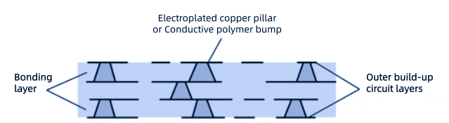
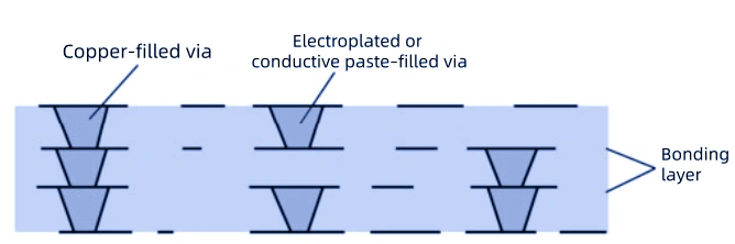
High-end HDI PCB interconnect technologies including copper-filled vias, conductive paste-filled vias, and copper pillar structures for enhanced reliability.
Laser drilling is constrained by physics. The thicker the copper foil, the higher the energy required for the laser to penetrate it.
Type III or ELIC structures undergo multiple high-temperature, high-pressure lamination cycles.
With signal rates surpassing 25Gbps, standard FR-4 materials may exhibit excessive loss in complex structures like Type III HDI. Consequently, Hybrid Stackups are becoming increasingly popular. This approach involves using high-frequency materials such as Rogers or Panasonic Megtron for critical signal layers, while using standard FR-4 for non-critical layers to balance performance and cost.
NextPCB has fully upgraded its capabilities to support hybrid lamination processes using Rogers high-frequency materials, catering to the needs of 5G and millimeter-wave radar applications.
Looking ahead, HDI technology will focus increasingly on environmental sustainability and extreme miniaturization. For a deeper analysis of future market and technical directions, please refer to our article: HDI PCB Trends 2026: Innovation, Market, and Sustainability.
| Stackup Type | Applicable BGA Pitch | Cost Factor | Manufacturing Difficulty | Recommended Applications |
|---|---|---|---|---|
| 1+N+1 (Type I) | > 0.65mm | Low | Low | Consumer electronics, Module boards |
| 2+N+2 (Type III) | 0.4mm - 0.65mm | Medium | Medium-High | High-end smartphones, Tablets, FPGA boards |
| ELIC / Any Layer | < 0.4mm | High | Very High | Flagship phones, Smart wearables |
Key Recommendations:
In hardware communities like r/PrintedCircuitBoard, High-Density Interconnect (HDI) is a frequent topic of debate. Most designers understand the "why" of HDI, but the "how"—specifically regarding stackup types like 1+N+1 and 2+N+2—often leads to confusion and unexpected manufacturing costs. As a manufacturer, we’ve gathered the most common questions from the community to help you bridge the gap between a great layout and a manufacturable board.
The numbers essentially count the sequential lamination cycles and laser drilling steps.
The price increase isn't just about adding more layers; it’s about process complexity. Each additional "+1" layer represents an entire cycle of lamination, laser drilling, desmear, copper plating (VCP), and imaging. A 2+N+2 board spends significantly more time on the production line. Furthermore, every lamination cycle introduces registration risks. Ensuring that a 0.1mm microvia aligns perfectly across multiple layers requires extreme precision, and the yield risk associated with that precision is factored into the cost.
If your design allows for it, Staggered Vias are always the better choice for reliability and cost.
While advanced LDI (Laser Direct Imaging) allows for extreme precision, we recommend staying at or above 3mil / 3mil (0.075mm) for standard HDI projects to maintain high yields and lower costs. We can push down to 2mil / 2mil, but this typically requires specialized thin copper foils and stricter etching controls, which will increase your per-board price.
You can often avoid HDI by optimizing your fan-out, but it becomes mandatory when:
The most frequent error is defining a via span that is physically impossible to manufacture in a single cycle. For example, a designer might define a microvia from Layer 1 to Layer 3 in a 1+N+1 stackup. In reality, that span requires a 2+N+2 process or a very deep laser drill that may violate aspect ratio rules. Always check your Drill Pair settings against the manufacturer's lamination sequence before you finish your routing.
At NextPCB, we provide comprehensive HDI manufacturing services ranging from standard 1+N+1 to complex ELIC structures. Leveraging advanced laser drilling equipment and deep expertise in material science, we ensure your designs are realized with precision.
>> This article references the IPC-2226-A Sectional Design Standard for High Density Interconnect (HDI) Printed Boards.

Image Disclaimer:
Some images in this article are sourced from the internet and used for technical illustration only. If any copyright issue arises, please contact us for removal or revision.
Still, need help? Contact Us: support@nextpcb.com
Need a PCB or PCBA quote? Quote now

