
 Surface


Stacy Lu

 NextPCB Capabilities
Printed Circuit Boards
NextPCB Capabilities
Printed Circuit Boards
 PCB Assembly
 Layer Buildup
 SMD-Stencils
 PCB Design-Aid & Layout
 Mechanics
 Quality
 Drills & Throughplating
 Factory & Certificate
 PCB Assembly Factory Show
Certificate
PCB Assembly Factory Show
Certificate
Support Team
Feedback:
support@nextpcb.com


The AI chip market in 2026 is more competitive than at any point in its history. NVIDIA GPUs dominate AI training with the H100, H200, and now B200—but that dominance is being challenged from every direction. Google's TPU v5 powers the majority of internal training at one of the world's largest AI research organizations. Amazon's Trainium 2, Cerebras's WSE-3, Groq's LPU, and dozens of other custom AI ASICs are claiming specific performance records and cost advantages. Intel's Gaudi 3 targets the open-standard OAM ecosystem. And FPGAs continue to hold territory in latency-sensitive inference and network processing applications.
For hardware engineers, infrastructure architects, and PCB designers, the question is not just which chip runs the best benchmark. It is which chip architecture creates the most demanding board-level design problem, which platform requires specialized manufacturing processes, and which will define the PCB requirements of AI server hardware through 2027 and beyond. Each architecture makes fundamentally different demands on the PCBs that carry it: the memory architecture differs, the interconnect topology differs, the power density differs, and the thermal management requirements differ correspondingly.
This article compares all four architectures—GPU, TPU, ASIC, and FPGA—systematically across compute throughput, power efficiency, PCB design requirements, software ecosystem, and total cost of ownership, concluding with a realistic assessment of which architecture is positioned to dominate each major AI workload category through 2027.
Before diving into the specifics, it helps to establish what each architecture actually is at the hardware level—not in marketing terms, but in terms of how computation is organized on silicon.
GPU (Graphics Processing Unit): A massively parallel processor originally designed for graphics rendering but redesigned over two decades for general-purpose parallel computation. A modern AI GPU contains tens of thousands of small arithmetic units (CUDA cores, Tensor Cores) that execute the same operation on many data elements simultaneously (SIMD/SIMT execution model). GPUs are programmable: they run arbitrary code written in CUDA or ROCm. Their generality comes at a cost in efficiency; a significant fraction of die area is devoted to control logic, caching, and scheduling overhead that a fixed-function accelerator does not need.
TPU (Tensor Processing Unit): A custom ASIC developed by Google specifically for the matrix multiplication operations that dominate deep learning. TPUs use a systolic array architecture: a grid of multiply-accumulate (MAC) units arranged so that data flows through the array in a wave pattern, with each unit passing its output to the next. This arrangement maximizes arithmetic throughput per die area for matrix operations but makes the chip less efficient for operations that do not fit the systolic pattern. TPUs are semi-programmable: they execute a limited set of tensor operations defined by Google's XLA (Accelerated Linear Algebra) compiler.
Custom AI ASIC (Application-Specific Integrated Circuit): A chip designed from scratch to execute a specific AI workload or family of workloads with maximum efficiency. ASICs for AI include Google's TPU (one category of ASIC), but also chips like Amazon's Trainium and Inferentia, Cerebras's WSE-3, Graphcore's IPU, and the growing field of startup inference chips. The defining characteristic is that the architecture is fixed at design time: the chip executes its target workload very efficiently but cannot be repurposed for workloads outside its design envelope without a new chip.
FPGA (Field-Programmable Gate Array): A chip containing a large array of configurable logic blocks and programmable interconnects that can be wired together after manufacture to implement any digital circuit. FPGAs are completely reprogrammable: the same physical chip can be reconfigured to implement a neural network accelerator, a network packet processor, or a digital signal processor by loading a different bitstream. FPGAs trade raw performance density for this flexibility: the configurable interconnect fabric consumes 70–80% of die area and introduces routing delays that fixed-function circuits do not have.
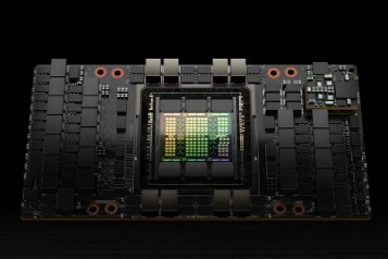
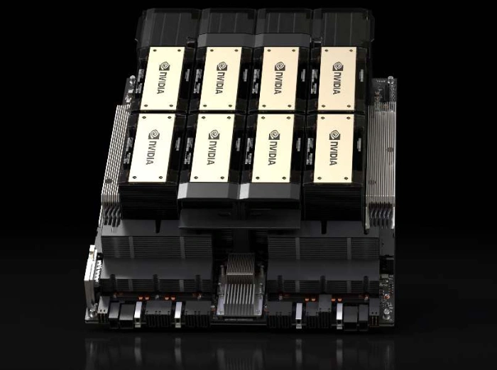
NVIDIA GPUs are the de facto standard for large-scale AI training in 2026, deployed in virtually every frontier AI training cluster worldwide. The reasons are straightforward: GPUs offer the highest absolute FP8 and BF16 throughput per chip, the most mature software ecosystem (CUDA), the best interconnect fabric for multi-GPU training (NVLink 5.0 at 1,800 GB/s per GPU in B200), and the widest support across all major AI frameworks.
The H100 SXM5 (989 BF16 TFLOPS dense) and B200 SXM6 (4,500 BF16 TFLOPS dense) represent the current and near-future peak of GPU performance for AI training. These numbers are not achieved on a single chip in isolation—they require high-bandwidth memory (HBM3/HBM3e), NVLink interconnects, and the NVSwitch-based all-to-all fabric described throughout the cluster and rack architecture covered in articles like the Blackwell Architecture guide and the GPU Rack Architecture guide.
GPU weaknesses are also well-defined. Their programmability requires substantial control hardware that consumes die area and power without contributing directly to tensor arithmetic. The large on-chip caches needed for general-purpose programming add die area and leakage power. And at 700–1,000 W per chip, GPU power density exceeds what most legacy data center infrastructure can support without dedicated power and cooling upgrades.
AMD's MI300X is the most significant GPU-class competitor to NVIDIA in the training and inference market, differentiated primarily by its 192 GB HBM3 capacity (vs 80 GB for H100 SXM5) and the OAM form factor that enables open infrastructure. The H100 vs MI300X comparison covers this trade-off in detail.
Google's Tensor Processing Units (TPUs) are the most mature non-GPU AI accelerator family, having been in production since 2016. TPU v5 (TPU v5e and v5p), introduced in 2023–2024, represents the current generation and is Google's primary training accelerator for internal workloads including the Gemini model family.
Architecture: TPUs use a matrix multiplication unit (MXU) based on a systolic array of MAC units. Each MAC unit performs a multiply-accumulate operation in INT8 or BF16 precision every clock cycle; data flows through the array in a wave so that each MAC unit receives operands from its neighbor rather than from a central register file. This eliminates the memory bandwidth bottleneck that limits GPU performance on compute-bound operations: once data enters the systolic array, it is reused without requiring additional memory accesses.
TPU v5p specifications (approximate):
TPU interconnect: Google's ICI provides high-bandwidth, low-latency all-to-all connectivity between TPU chips in a pod, similar in function to NVLink but implemented in Google's proprietary fabric. TPU v5p pods scale to 8,960 chips per pod, connected in a 3D torus topology. The ICI links are routed on the PCB of Google's custom TPU server boards, with signal integrity requirements comparable to NVLink 4.0.
Key limitation: TPUs are only available through Google Cloud (or via Google's internal compute allocation). There is no ability to purchase TPUs for on-premises deployment. Organizations whose AI strategy requires on-premises infrastructure or multi-cloud flexibility must use GPUs or alternative ASICs.
Custom AI ASICs represent the most diverse category in this comparison, encompassing chips from dozens of vendors targeting different workloads, precision tiers, and deployment scenarios. The common thread is that each ASIC sacrifices programmability for efficiency: by designing the chip specifically for its target workload, the designer eliminates the control overhead, cache hierarchy, and scheduling logic that a general-purpose processor requires.
Amazon Trainium 2: Amazon's second-generation training accelerator, deployed in AWS Trn2 instances. Trainium 2 uses a novel NeuronCore architecture with dedicated matrix multiply engines and collective compute units that execute all-reduce operations in hardware rather than in software. In a 16-chip Trn2 server, Trainium 2 chips are connected by Amazon's proprietary NeuronLink v2 at up to 1,600 GB/s aggregate bandwidth per chip. PCB-level, Trainium 2 uses standard PCIe Gen5 for host connectivity and a custom high-bandwidth interconnect between chips that imposes similar signal integrity requirements to NVLink 4.0.
Cerebras WSE-3: The most unconventional AI chip architecture currently in production. The Wafer-Scale Engine 3 is a single die occupying an entire 300 mm wafer, containing 900,000 AI cores and 44 GB of on-wafer SRAM. By placing all computation and memory on a single die without off-chip memory accesses for on-chip operations, the WSE-3 eliminates the memory bandwidth bottleneck entirely for models that fit within its 44 GB SRAM. For large models that exceed this capacity, off-chip memory access is required. The WSE-3 PCB is unique: a single 12” (305 mm) silicon die mounted on a custom carrier board with a massive power delivery infrastructure (15 kW per chip) and liquid cooling mandatory. There is no comparable PCB design problem in commercial electronics.
Graphcore IPU (Intelligence Processing Unit): Graphcore's IPU uses a Bulk Synchronous Parallel (BSP) execution model where all processing elements execute independently for a defined time step, then exchange data in a synchronized communication phase. This architecture is well-suited to graph neural networks and sparse AI workloads but less efficient than GPUs on dense transformer operations. The PCB design for IPU-based servers is less extreme than GPU servers: IPUs consume 180–250 W per chip and use PCIe Gen4 host connectivity, placing them in a moderate PCB complexity tier.
Groq LPU (Language Processing Unit): Groq's LPU is designed specifically for LLM inference at high token throughput and low latency. Its architecture uses deterministic execution (no caches, no branch prediction, no out-of-order execution) with all computation mapped statically to hardware resources at compile time. This determinism enables extremely consistent, low-latency token generation but limits flexibility for training or non-transformer workloads. Groq deploys LPUs in dense server configurations with LPDDR5 memory on-package, minimizing PCB memory routing complexity.
FPGAs occupy a niche in AI infrastructure that is both well-defined and resilient: applications where the workload changes frequently, where latency requirements are more stringent than GPU schedulers can reliably meet, or where the volume is too small to justify a custom ASIC.
Leading FPGA vendors for AI applications include Intel (Stratix, Agilex series) and AMD/Xilinx (Versal, UltraScale+ series). Modern AI-optimized FPGAs include hardened DSP blocks, HBM or LPDDR5 memory interfaces, and PCIe Gen4/Gen5 connectivity. Their peak INT8 inference throughput is approximately 50–500 TOPS depending on device size—orders of magnitude below a GPU or dedicated ASIC, but achieved at 25–100 W TDP.
The primary AI applications for FPGAs in 2026 are:
PCB design for FPGA-based AI systems is typically less demanding than GPU boards because FPGA TDPs are lower (25–100 W for AI inference FPGAs vs 700–1,000 W for GPU), memory interfaces use DDR5 or LPDDR5 rather than HBM (lower PCB routing complexity), and the PCIe host interface is Gen4 or Gen5 rather than proprietary high-speed links. Layer counts of 8–16 are typical for FPGA AI inference boards.
| Architecture | Representative Chip | BF16 Training (TFLOPS) | INT8 Inference (TOPS) | FP64 HPC (TFLOPS) | TDP (W) |
|---|---|---|---|---|---|
| GPU (NVIDIA) | H100 SXM5 | 989 (dense) | ~3,958 | 34 | 700 |
| GPU (NVIDIA) | B200 SXM6 | 4,500 (dense) | ~18,000 | ~90 | 1,000 |
| GPU (AMD) | MI300X | 1,307 (dense) | ~2,614 | 163 | 750 |
| TPU | TPU v5p | ~459 | ~918 (INT8) | N/A | ~450 |
| Custom ASIC | Trainium 2 | ~3,200 (est.) | N/A (training-focused) | N/A | ~700 |
| Custom ASIC | Cerebras WSE-3 | ~125,000 (model-dependent) | Very high (SRAM-resident models) | N/A | ~15,000 |
| FPGA | AMD Versal Premium | N/A (not suited for training) | ~300–500 (INT8) | N/A | ~100 |
Raw TFLOPS comparisons are inherently misleading because different architectures achieve different fractions of theoretical peak on real workloads. A GPU at 40% model FLOP utilization (MFU) on LLaMA-3 training may outperform a TPU at 60% MFU on the same model if the GPU's peak TFLOPS are high enough to compensate. Meaningful performance comparisons require end-to-end benchmarks on representative workloads at realistic batch sizes—a complex empirical question that changes as compilers and software frameworks evolve.
Quick answer: Custom inference ASICs can reach up to 10× better TOPS-per-watt than an NVIDIA H100 GPU on fixed transformer inference workloads (see table below) — near, but not always a full order of magnitude. TPUs, by contrast, are not dramatically more power-efficient per chip than GPUs; their advantage is software/system-level, not raw silicon efficiency.
Power efficiency (TOPS per Watt or TFLOPS per Watt) is as important as raw throughput for data center economics, because power and cooling infrastructure are often the binding constraint on AI cluster scale, not GPU procurement cost. At 120 kW per GB200 NVL72 rack and typical data center PUE of 1.3, the annual electricity cost for a single rack exceeds $150,000–$200,000 at US commercial electricity rates.
| Architecture / Chip | INT8 Inference TOPS | TDP (W) | INT8 TOPS/W | Relative Efficiency |
|---|---|---|---|---|
| NVIDIA H100 SXM5 | ~3,958 | 700 | ~5.7 | 1.0× (baseline) |
| NVIDIA B200 SXM6 | ~18,000 | 1,000 | ~18.0 | 3.2× |
| AMD MI300X | ~2,614 | 750 | ~3.5 | 0.6× |
| Google TPU v5e | ~918 | ~197 | ~4.7 | 0.8× |
| Custom inference ASIC (est.) | 2,000–10,000+ | 100–300 | 10–50+ | 2–9× |
| FPGA (AMD Versal) | ~400 | ~100 | ~4.0 | 0.7× |
Custom inference ASICs show dramatically better TOPS per Watt than GPUs because they are designed exclusively for inference at specific precision tiers (INT8, INT4, FP8) without the power overhead of GPU general-purpose control logic, floating-point units for FP64, or large cache hierarchies. The trade-off is that these efficiency gains only materialize on the specific workload and model architectures the ASIC was designed for; if the target model changes significantly, the ASIC may require a new design generation.
Each AI chip architecture creates a distinct set of PCB design requirements, driven by its memory architecture, interconnect topology, power density, and form factor. The following table summarizes the key PCB design parameters for each architecture category.
| PCB Parameter | GPU (H100/B200) | TPU (v5) | Custom ASIC (varied) | FPGA (AI inference) |
|---|---|---|---|---|
| Typical board layer count | 20–32+ | 16–24 (est.) | 8–28 (wide range) | 8–16 |
| Memory interface on PCB | None (HBM on package) | None or HBM on package | DDR5, LPDDR5, or HBM on package | DDR5 or LPDDR5 on board |
| Host interface | PCIe Gen5/Gen6; NVLink | PCIe Gen4/5; ICI (proprietary) | PCIe Gen4/5 (most); proprietary links | PCIe Gen4/5 |
| Inter-chip interconnect on PCB | NVLink 4.0/5.0 at 100–200 Gb/s per lane | ICI at ~4,800 Gb/s aggregate | Proprietary (Trainium: NeuronLink; Groq: none) | None (single-chip for most AI inference) |
| Signal layer laminate | Megtron 6E / Megtron 7 | Megtron 6E class (est.) | FR4 to Megtron 7 depending on speed | Megtron 6 or FR4 |
| Copper foil | VLP to HVLP | VLP (est.) | LP to HVLP depending on interconnect speed | LP or standard ED |
| Power per chip (TDP) | 700–1,000 W | 197–450 W | 15 W to 15,000 W (WSE-3) | 25–100 W |
| Cooling requirement | DLC mandatory (B200); strongly preferred (H100) | DLC preferred at v5p power levels | Air to DLC depending on TDP | Air cooling adequate |
| HDI via technology | 2+N+2 to any-layer HDI (ELIC) | HDI (estimated) | Standard to HDI depending on package | Standard through-hole or 1+N+1 HDI |
| PCB manufacturing complexity | Very high (industry frontier) | High | Low to very high (wide range) | Low to moderate |
GPU boards, as detailed throughout the HDI PCB layer count guide and the AI Accelerator PCB Design Guide, set the current frontier of commercial PCB complexity. Custom inference ASICs span the widest range—from a simple 8-layer board for a low-power edge inference chip to the extraordinary WSE-3 carrier board at 15 kW. FPGAs represent the most accessible end of the spectrum for PCB engineers more accustomed to enterprise server designs.
Software ecosystem maturity is arguably the most durable competitive advantage any AI chip can have, because the cost of migrating a production AI pipeline from one chip to another is measured in months of engineering effort, not just hardware procurement dollars.
| Architecture | Primary SDK/Framework | PyTorch Support | Custom Kernel Dev | Migration from CUDA |
|---|---|---|---|---|
| NVIDIA GPU | CUDA; cuDNN; TensorRT | Native; deepest optimization | CUDA C++; PTX; Triton | N/A (CUDA is the reference) |
| AMD GPU | ROCm; HIP; MIOpen | Production-quality ROCm backend | HIP (CUDA-like API); HIPIFY tools | Moderate; HIPIFY automates ~80% |
| Google TPU | JAX + XLA; TensorFlow | PyTorch/XLA backend (production) | XLA/MLIR; limited vs CUDA | Significant (different programming model) |
| Amazon Trainium | Neuron SDK; NxD (NeuronX Distributed) | PyTorch Neuron plugin | Limited; Neuron kernel library | Significant; Neuron SDK compilation required |
| Cerebras WSE | Cerebras Software Platform (CSP) | PyTorch; TensorFlow via CSP | Limited to CSP framework | Significant; model must fit CSP memory model |
| FPGA | Vitis AI (AMD); OpenVINO (Intel) | Limited; custom compilation required | Full hardware design (VHDL/Verilog/HLS) | Very high; hardware design skill required |
CUDA's 15-year head start means that virtually every public AI model, research paper implementation, and production inference framework was written for CUDA first. The labor cost of porting a production LLM serving stack to a non-CUDA platform is substantial; organizations without CUDA-dependent codebases or with sufficient engineering resources to absorb the migration cost are the primary candidates for non-GPU platforms.
List price comparisons between AI chip platforms are complicated by limited public pricing, cloud-only availability for some platforms, and the rapid depreciation of AI hardware. A more useful framework is total cost of ownership (TCO) per unit of AI work, which includes hardware acquisition, power, cooling, and software/labor costs.
Several factors drive TCO differences across architectures:
| Use Case | Best Fit Architecture | Alternative | Why |
|---|---|---|---|
| Frontier LLM pre-training (> 70B parameters) | GPU (NVIDIA B200 / H100) | TPU v5p (Google internal) | Highest absolute throughput; NVLink 5.0 enables efficient tensor parallelism at scale |
| LLM fine-tuning (7B–70B) | GPU (H100 / MI300X) | Trainium 2 (AWS users) | Adequate memory, mature fine-tuning software (LoRA, DPO), competitive cost |
| LLM inference (< 70B, high throughput) | GPU (H100 PCIe / MI300X) | Custom inference ASIC (Groq, proprietary) | Software ecosystem, model compatibility; ASIC competitive for specific models |
| LLM inference (70B–180B, memory-bound) | GPU (MI300X / H200) | GPU (B200) | 192 GB HBM capacity fits large models on single GPU; reduces tensor parallelism overhead |
| Ultra-low-latency inference | Custom ASIC (Groq LPU) | FPGA | Deterministic execution; no scheduler jitter; < 1 ms time-to-first-token achievable |
| Vision model inference (production scale) | GPU (A10G / L40S) | Custom ASIC, FPGA | Mature TensorRT optimization for CNN/ViT; acceptable cost at moderate scale |
| Scientific HPC + AI | AMD MI300X | NVIDIA H100 | MI300X 163 TFLOPS FP64 vs H100's 34 TFLOPS; MI300X dominates FP64 HPC workloads |
| Network AI (packet processing) | FPGA or SmartNIC ASIC | GPU (not ideal) | Line-rate packet processing requires deterministic, line-rate hardware; GPUs cannot match FPGA latency |
| Edge inference (< 10 W) | Custom ASIC (NPU, embedded) | FPGA (low-volume) | Dedicated neural processing units in edge SoCs provide orders-of-magnitude better TOPS/W than GPU at this power level |
| AI chip prototyping | FPGA | N/A | Reprogrammable hardware enables architecture validation before ASIC tape-out at $10M–$100M cost |
Predicting semiconductor market dominance is inherently uncertain, but the structural forces shaping the AI chip landscape through 2027 are clear enough to make directional assessments with reasonable confidence.
GPUs will continue to dominate training. NVIDIA's GPU platform has three structural advantages that no competitor has closed: the CUDA software ecosystem (15+ years of accumulated optimization), the NVLink/NVSwitch interconnect fabric (the only commercial solution for rack-scale fully-connected GPU training), and the breadth of model support (every publicly released model runs on CUDA). AMD MI300X is the most credible training alternative, but primarily for FP64 HPC workloads and cost-sensitive large-model inference rather than frontier pre-training. By 2027, NVIDIA B200 and the anticipated Rubin (R100) generation will extend the GPU performance lead in training, and the NVL72 architecture will likely be extended to even larger rack-scale configurations.
Custom inference ASICs will gain significant market share in specific serving use cases. The economics of LLM inference at scale favor purpose-built chips: a custom INT8 or FP8 inference ASIC at 10–50 TOPS/W is 3–10× more power-efficient than an H100 for fixed-architecture inference workloads. As LLM architectures stabilize (the transformer architecture shows no sign of being displaced), the economics of building a chip tuned specifically for transformer inference become increasingly attractive. Amazon Trainium/Inferentia, Google's TPU for serving, and a growing ecosystem of inference startup chips will collectively capture a meaningful fraction of the LLM inference market that currently runs on GPUs.
FPGAs will remain in their niches. The FPGA market for AI will not expand dramatically through 2027 because the performance/watt of FPGAs on typical neural network operations remains below purpose-built ASICs and competitive GPUs. FPGAs will remain dominant in ultra-low-latency inference (financial HFT), network AI (SmartNICs), and pre-ASIC prototyping. The programmability advantage of FPGAs over ASICs will be maintained, but the performance gap versus GPUs and inference ASICs will not close materially.
PCB engineering implications for 2027: The dominant PCB design challenges through 2027 will continue to be defined by GPU boards—specifically, B200 and next-generation GPU baseboards at 24–32 layers, Megtron 7 with HVLP copper, and NVSwitch 4.0 boards at 32–40+ layers with any-layer HDI. Custom inference ASIC boards will grow as a category but remain heterogeneous in requirements. FPGA boards will continue at moderate complexity. The trajectory described in articles like the Blackwell Architecture guide and the discussions of NVLink 5.0 requirements in the NVLink PCB routing guide represents the direction the industry is moving, not a temporary peak.
Is a custom AI ASIC an order of magnitude more power-efficient than a GPU for transformer inference?
Close, but not a full order of magnitude across the board. Per the efficiency comparison above, the most efficient custom inference ASICs reach up to 10× better TOPS/W than an H100 on fixed transformer inference workloads—approaching but not exceeding a true 10× gain—while typical designs land in the 3–9× range depending on precision tier and workload fit. Treat any flat “order of magnitude” claim as an upper-bound best case, not a guaranteed multiplier.
Is Google's TPU an ASIC, not a GPU?
Yes. A TPU is a custom ASIC that Google designed specifically for matrix multiplication using a systolic array architecture—it is not a general-purpose GPU. Per-chip, TPU v5e's measured power efficiency (~4.7 INT8 TOPS/W) is not dramatically higher than an H100 GPU's (~5.7 TOPS/W); TPU's efficiency advantage mainly comes from system-level utilization on Google's XLA software stack, not a raw per-chip order-of-magnitude gap.
Can an FPGA replace a GPU for AI training?
Not practically. Modern GPU training boards achieve 989 TFLOPS (H100) to 4,500 TFLOPS (B200) in BF16 at 700–1,000 W TDP. The largest production FPGAs achieve approximately 100–500 INT8 TOPS at 75–150 W—roughly 10–30× lower throughput per chip at lower power. An FPGA cluster large enough to match a single H100's training throughput would consume more board space, power, and total cost than the GPU solution while offering no software compatibility with PyTorch or existing CUDA training code. FPGAs are suited to inference, prototyping, and specialized fixed-function compute—not large-scale neural network training.
Is Google's TPU faster than NVIDIA's H100?
On Google's own benchmark workloads (training Gemini and related models using JAX/XLA), TPU v5p achieves competitive or superior performance to H100 within Google's infrastructure. However, TPU v5p at ~459 BF16 TFLOPS peak is lower than H100's 989 TFLOPS; TPU's advantage comes from very high hardware utilization on workloads compiled with Google's XLA compiler and run on TPU-native frameworks. For organizations using PyTorch and standard open-source models, H100 is generally faster and requires no migration effort. TPUs are only accessible via Google Cloud, limiting their applicability for on-premises or multi-cloud deployments.
What makes a custom ASIC more efficient than a GPU for inference?
A custom inference ASIC can eliminate all hardware that a GPU includes for general-purpose programming—branch predictors, out-of-order execution engines, large L2/L3 caches, floating-point units for precision tiers not needed for the target model, and general-purpose scheduling logic. For a fixed transformer inference workload in INT8, these elements represent 30–50% of GPU die area and a significant fraction of its power consumption. By dedicating that area and power entirely to INT8 matrix multiply units and the specific memory access patterns of transformer inference, a well-designed ASIC can achieve 3–10× better TOPS/W on its target workload. The trade-off is that this efficiency disappears if the workload changes significantly from the design target.
Why do GPU PCBs require so many more layers than FPGA boards?
GPU boards require high layer counts primarily because of NVLink routing: a DGX H100 baseboard routes thousands of NVLink 4.0 differential pairs at 100 Gb/s per lane between 8 GPU packages and 4 NVSwitch chips, requiring 6–10 dedicated high-speed signal routing layers plus adjacent ground reference planes. FPGA AI inference boards have no equivalent interconnect: the FPGA is typically a single chip connected to the host via PCIe, with DDR5 memory on-board. Without the multi-chip NVLink routing challenge, FPGA boards can achieve adequate performance with 8–16 layers of standard or moderately low-loss material.
Will the NVIDIA GPU monopoly on AI training persist through 2027?
NVIDIA's GPU platform will remain dominant for frontier AI training through 2027 based on its CUDA software ecosystem, NVLink interconnect advantage, and the B200/Rubin performance roadmap. However, “dominant” does not mean “exclusive”: AMD MI300X is winning cost-sensitive large-model inference workloads, Google TPU v5 continues to power internal AI training at scale, and Amazon Trainium is growing within AWS deployments. By 2027, NVIDIA's market share in AI accelerators will likely be lower than 2024’s peak, but the company will retain leadership in the frontier training segment that commands the highest revenue per chip.
Which AI chip architecture has the best PCB design documentation for engineers?
NVIDIA GPU boards have by far the most publicly available PCB design documentation, primarily because NVIDIA's HGX and OAM-adjacent partner programs have generated a large body of application notes, reference designs, and third-party analysis. AMD MI300X OAM-format boards benefit from the OCP's open OAM specification, which provides a published electrical and mechanical interface standard that any PCB designer can reference. TPU, custom ASIC, and FPGA AI boards typically have proprietary reference designs that are not publicly documented. For PCB engineers entering the AI server hardware space, the GPU ecosystem provides the most accessible starting point for design learning.
Whether you are designing GPU baseboards for H100 or B200, OAM Universal Base Boards for MI300X deployments, custom inference ASIC carrier boards, or FPGA-based AI inference cards, NextPCB supports the full spectrum of AI accelerator PCB requirements—from 8-layer FPGA inference boards through 32-layer NVSwitch HDI designs. Our capabilities include ultra-low-loss laminate processing, HVLP copper foil, high-layer-count fabrication, BGA assembly, 3D X-ray inspection, and IPC Class 3 standards for the complete AI hardware supply chain.

Still, need help? Contact Us: support@nextpcb.com
Need a PCB or PCBA quote? Quote now

