

 NextPCB Capabilities
 PCB Assembly
 Layer Buildup
 SMD-Stencils
 PCB Design-Aid & Layout
 Mechanics
 Surface
 Quality
 Drills & Throughplating
 Factory & Certificate


BGA packages don't expose their solder joints. Neither do QFNs, bottom-terminated components, or anything sitting beneath an RF shield. Once a board comes off the reflow oven, a significant portion of its solder connections are physically inaccessible to any camera — and those are exactly the joints most likely to carry process defects that won't show up until the product is already in the field.
At NextPCB, we've invested in a specific X-Ray configuration designed to handle the full complexity of modern PCBA production. This article explains why X-Ray inspection matters at the assembly stage, breaks down the exact equipment and capabilities we use, and shows how that investment translates into tangible quality assurance for every board we build.
Why X-Ray Inspection Is Essential at the PCBA Stage
As PCBs become denser and components like BGAs (Ball Grid Arrays) and QFNs hide their solder joints completely beneath their packages, traditional Automated Optical Inspection (AOI) simply cannot do the job alone. X-Ray inspection has become an indispensable line of defense at the PCBA stage — and how well it's implemented directly determines whether a finished board is truly reliable or a field failure waiting to happen.
Once a bare PCB goes through SMT pick-and-place and reflow soldering, a new category of defects becomes possible — ones that no camera can detect. BGA packages have solder balls hidden directly beneath the component body. QFN pads are flush against the board surface. Over-molded connectors and components beneath RF shields are completely opaque to optical systems.
https://nepp.nasa.gov/docuploads/06AA01BA-FC7E-4094-AE829CE371A7B05D/NASA-STD-8739.3.pdf
The defects that hide in these locations are also among the most consequential:
- Solder voids — gas bubbles trapped inside BGA balls that reduce thermal and electrical conductivity, and accelerate joint fatigue under thermal cycling.
- Bridging — unintended solder connections between adjacent pads, invisible beneath component bodies.
- Cold joints and head-in-pillow defects — joints that appear formed but are not properly fused, which often pass visual inspection but fail in the field.
- Missing or misaligned balls — individual BGA balls that didn't reflow correctly or are entirely absent.
X-Ray inspection penetrates through component housings and solder masks to image these joints directly — non-destructively, in real time, and at production speed. Many manufacturers use a 25% voiding threshold as a practical acceptance guideline for BGA solder joints, although acceptance criteria may vary depending on package type, application requirements, and IPC-A-610 standards. Only X-Ray can measure that reliably at scale.
The table below summarizes how X-Ray compares to the other two inspection methods commonly used in PCBA production — Automated Optical Inspection (AOI) and In-Circuit Test (ICT) — and shows why each method covers different ground rather than substituting for one another.
| Inspection Method | What It Can Detect | What It Cannot Detect | Applicable Stage |
|---|---|---|---|
| AOI (Automated Optical Inspection) | Missing components, wrong polarity, visible solder bridges, skewed placements, insufficient solder on exposed pads | Any defect hidden beneath a component body — BGA voids, QFN bridging, PTH barrel fill | Post-placement / post-reflow |
| X-Ray Inspection | BGA solder voids and ball collapse, hidden bridging under QFN/BGA, PTH barrel fill depth, head-in-pillow defects, cold joints beneath packages | Functional electrical defects, component value errors, opens in inaccessible nets | Post-reflow / final assembly |
| ICT (In-Circuit Test) | Opens, shorts, wrong component values, parametric faults on accessible test points | Solder joint internal structure, voiding, physical defects with no electrical signature yet | Post-assembly (requires test fixture) |
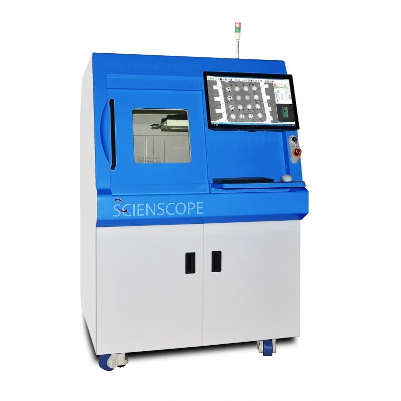
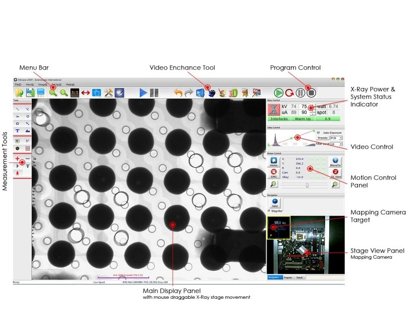
NextPCB's Configuration: The SCIENSCOPE X-SCOPE-2000
For PCBA production inspection, NextPCB operates the SCIENSCOPE X-SCOPE-2000 X-Ray Cabinet Inspection System. This is a mid-to-high-tier industrial inspection platform positioned between entry-level 2D systems and laboratory-grade CT scanners — a deliberate choice that balances resolution, throughput, and cost-effectiveness for real production environments.
Here is a detailed breakdown of the system's specifications and why each feature matters in practice:
5-Micron Closed X-Ray Tube (90kV / 110kV)
The X-SCOPE-2000 uses a closed, maintenance-free X-Ray tube with a 5-micron focal spot size, operating at up to 90kV (with a 110kV option available). The focal spot size is arguably the most important specification in any X-Ray inspection system — it directly determines the sharpness and resolution of the resulting image.
A 5-micron spot means that many solder voids, bridges, missing balls, and some larger crack-related defects, hairline bridges between pads, and subtle voids within individual BGA balls are rendered with clarity. The closed tube design eliminates the need for periodic filament replacement, reducing downtime and ensuring consistent performance across the system's operational life.
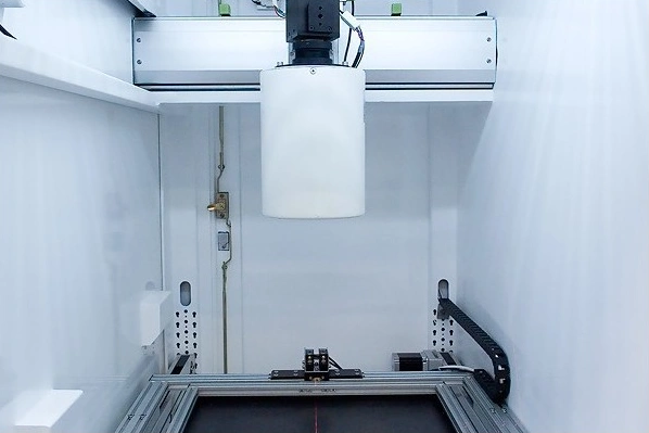
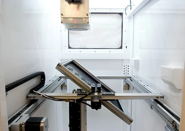
70-Degree Oblique Angle Viewing
Standard 2D X-Ray systems image the board from directly above. This creates a fundamental problem: components and solder joints on the top and bottom layers of a board overlap in the image, making it difficult to isolate defects on either side. Tall components cast shadows that obscure the joints beneath them.
The X-SCOPE-2000 addresses this with a mechanical tilting stage that rotates to 70 degrees, enabling oblique-angle imaging. By viewing BGA balls and PTH (Plated Through-Hole) barrel fills from an extreme angle, our QA engineers can effectively separate top-layer and bottom-layer features, inspect barrel fill depth in through-hole joints, and examine the profile of BGA solder balls in a way that helps identify potential head-in-pillow indications and partial collapse. The oblique-angle capability provides a more three-dimensional view of solder structures compared with conventional top-down 2D imaging.
14-Bit Digital Flat Panel Detector at 30fps
Image quality in X-Ray inspection is determined not only by the tube, but by the detector. The X-SCOPE-2000 is equipped with a 14-bit digital flat panel detector, which captures 16,384 distinct grayscale levels at 30 frames per second.
This dynamic range matters enormously when differentiating between materials of varying density within a single image — for example, distinguishing a small void from dense solder, or separating a copper pad from a lead-free solder ball. Voiding percentage calculations, which NextPCB reports against the IPC-A-610 25% threshold, depend directly on the detector's ability to resolve subtle density gradients accurately.
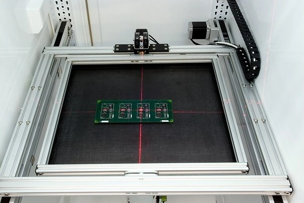
22" × 21" Programmable X-Y Stage
The inspection stage measures 22 inches by 21 inches and is fully programmable with variable-speed X-Y motion. This accommodates everything from small IoT modules to large server motherboards or multi-panel SMT arrays without requiring fixturing changes. Programmable inspection routines mean that once a recipe is established for a given board layout, every subsequent board in the production run is inspected consistently and automatically — eliminating operator-to-operator variability.
Megapixel Mapping Camera and Software Interface
Alongside the X-Ray detector, the system integrates a high-resolution optical mapping camera. This allows engineers to correlate X-Ray imagery with visible-light images of the board, enabling faster defect localization, more precise reporting, and easier cross-referencing with assembly drawings or Gerber data during First Article Inspection (FAI).
The X-SCOPE-2000 software brings all control surfaces together in a single interface: live X-Ray display with mouse-draggable stage movement, real-time X-Ray power and system status readouts, video enhancement tools, programmable motion control, and a stage-view panel from the mapping camera. Engineers can switch between the X-Ray image and the optical reference view instantly — a practical advantage when correlating a detected void to a specific component reference designator on the board.
How NextPCB Applies This Technology in Production
BGA and QFN Joint Inspection
Every BGA on an assembled board goes through a programmed inspection routine using the X-SCOPE-2000. Our engineers calculate the voiding percentage of individual solder balls and compare them against the IPC-A-610 acceptance criteria. Boards with any ball exceeding the 25% void threshold are flagged, reviewed, and either reworked or rejected before leaving our facility. Critical BGAs are inspected according to your project requirements and internal quality procedures.
First Article Inspection (FAI)
The first board off a production run is subjected to comprehensive X-Ray inspection to verify that the SMT reflow profile, paste volume, and component placement have produced acceptable joint formation across the entire board. Any deviations caught at FAI are corrected before the rest of the batch proceeds — catching process issues early rather than at final test.
While IPC-A-610 remains the primary acceptability standard for commercial electronics assembly, high-reliability industries often reference additional workmanship standards. NASA's NASA-STD-8739.3 Soldered Electrical Connections provides detailed guidance on solder joint integrity, inspection requirements, and workmanship practices for mission-critical electronic hardware.
Complex and Shielded Assembly Verification
For boards with RF shields, over-molded connectors, stacked packages, or other features that block optical access, X-Ray is the only practical inspection tool. The penetration capability of the 90kV tube ensures that no joint is left uninspected simply because of the component packaging surrounding it.
PTH Barrel Fill Verification
Through-hole components are wave-soldered or hand-soldered, and IPC standards specify minimum barrel fill requirements for structural integrity. The 70-degree tilt capability of the X-SCOPE-2000 allows our engineers to directly image barrel fill in PTH joints — a check that is otherwise difficult to verify non-destructively the board.
X-Ray at the PCBA Stage vs. X-Ray in Bare Board Fabrication
It's worth clarifying a distinction that sometimes creates confusion: X-Ray is used at two completely different stages of the electronics manufacturing process, and the machines involved serve entirely different purposes.
During bare PCB fabrication — specifically after the lamination of multi-layer boards — manufacturers use X-Ray Target Drilling Systems to locate hidden inner-layer copper fiducials and drill mechanical alignment holes through them. These are production machines that physically alter the board. They prioritize drilling accuracy and units-per-hour throughput.
At the PCBA stage, the purpose is entirely different: non-destructive testing. Nothing is drilled or modified. The board passes through the X-Ray cabinet, is imaged, evaluated, and released or rejected. The table below summarizes the key differences between these two applications of X-Ray technology.
| Characteristic | X-Ray in Bare PCB Fabrication | X-Ray in PCBA Inspection |
|---|---|---|
| Primary purpose | Locate hidden inner-layer fiducials and drill physical alignment holes | Detect hidden solder defects non-destructively |
| Stage in process | After multi-layer lamination, before outer-layer processing | After SMT reflow soldering and component assembly |
| Effect on board | Physically alters the board — drills holes | No physical alteration — purely imaging and evaluation |
| Machine category | Production / machining equipment | Non-Destructive Testing (NDT) equipment |
| Key performance metrics | Drilling positional accuracy, units per hour (UPH) | Focal spot size (resolution), tilt angle range, detector dynamic range |
| Output | Drilled reference holes aligned to inner copper targets | X-Ray images, voiding reports, pass/fail records per IPC-A-610 |
Understanding this distinction helps clarify why the investment in the right PCBA-stage X-Ray system is separate from, and complementary to, the quality of the bare boards being assembled.
What This Means for Your Project
Choosing an EMS partner based on price alone carries risk that doesn't always show up until boards are in the field. Hidden solder defects — the kind that only X-Ray can detect — are responsible for a significant share of electronics field failures, warranty returns, and product recalls. By the time they surface, the cost of remediation is orders of magnitude higher than the cost of proper inspection during production.
When you manufacture with NextPCB, our X-Ray inspection process is integrated into the standard production workflow — not an optional add-on. The SCIENSCOPE X-SCOPE-2000 configuration described in this article is what runs on our floor, and it means that BGAs, QFNs, shielded assemblies, and through-hole joints are all verified against IPC-A-610 standards before your boards ship. For a full picture of what our lines support — including SMT, BGA, and THT process specifications — see our PCBA assembly capabilities page.
For more detail on how X-Ray inspection fits within the broader IPC-A-610 acceptability framework, the IPC's official documentation is a useful reference. For information on the SCIENSCOPE X-SCOPE-2000 system specifications, the SCIENSCOPE website provides full technical details.
Get a PCBA Quote with X-Ray Inspection Included
Whether you're building a prototype run of 10 boards or scaling to high-volume production, NextPCB's assembly process supports the X-Ray inspection infrastructure needed to back every board with documented quality assurance.
Get an instant online PCBA quote — and build with the confidence that comes from knowing exactly what's inside every joint.
If you're at the earliest stage of a new design, Rev 0 PCBA is NextPCB's no-touch prototype service built specifically for first-spin boards — handling PCB fabrication and assembly together so your Rev 0 arrives ready to test, with the same X-Ray inspection coverage applied from the very first unit.
Frequently Asked Questions (FAQ) about PCBA X-Ray Inspection
1. Does NextPCB perform X-Ray inspection on every board, and does it cost extra?
At NextPCB, X-Ray inspection is integrated into our standard Quality Assurance (QA) workflow for all designs containing BGAs, QFNs, and other bottom-terminated components. For prototype and first-article runs, we inspect 100% of these critical joints. For large-scale production, we perform batch-sampling inspections based on IPC standards. This service is included as part of our rigorous assembly quality control, meaning there are no hidden "add-on" fees for standard project configurations.
2. Can X-Ray radiation damage sensitive components like Flash memory, MCUs, or sensors?
No, the X-Ray levels used in PCBA inspection are completely safe for standard silicon-based components. The SCIENSCOPE X-SCOPE-2000 operates at relatively low energy levels (90kV to 110kV) with extremely short exposure times. This dosage is several orders of magnitude below the threshold required to cause lattice displacement or charge-trapping issues in modern non-volatile memories, microcontrollers, or MEMS sensors. Your hardware is completely safe.
3. What happens if a solder joint exceeds the 25% BGA voiding threshold? Do you automatically rework it?
If our QA engineers detect a voiding percentage exceeding 25% (or any other anomaly like bridging or head-in-pillow defects), the board is automatically flagged and routed to our specialized SMT rework station. We utilize precision BGA rework systems to safely de-solder, clean, re-ball (if necessary), and re-solder the component. After rework, the board must pass a secondary X-Ray inspection to verify joint integrity before it can be approved for shipment.
4. I have BGAs placed directly opposite each other on both sides of the PCB. Can your X-Ray system still inspect them?
Yes. Overlapping BGAs on double-sided assemblies are notoriously difficult to inspect with standard top-down 2D X-Ray systems, as the top and bottom solder balls merge into a single shadow. However, our system's 70-degree oblique angle viewing allows us to tilt the stage and isolate the solder joints of each layer independently. By changing the viewing angle, we can clearly distinguish the upper-side BGA balls from the lower-side ones to measure voiding and check for bridges.
5. Can I request the raw X-Ray images or a formal QA inspection report for my project?
Absolutely. We provide comprehensive inspection reports upon request. During the checkout process or through your dedicated NextPCB account manager, you can request the First Article Inspection (FAI) report or specific X-Ray imaging data for your BGA/QFN components. This documentation is highly recommended for industrial, medical, or aerospace-grade projects that require strict traceability.

