

 Printed Circuit Boards
 Surface
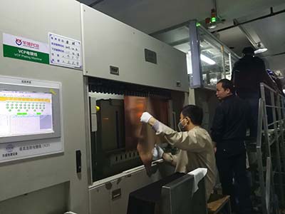
 PCB Assembly
 Layer Buildup
 Online Tools
 PCB Design-Aid & Layout
 Mechanics
 SMD-Stencils
 Quality
 Drills & Throughplating
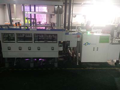
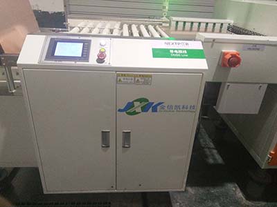
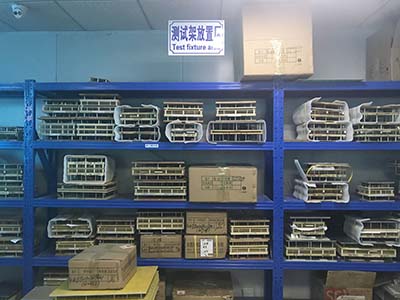
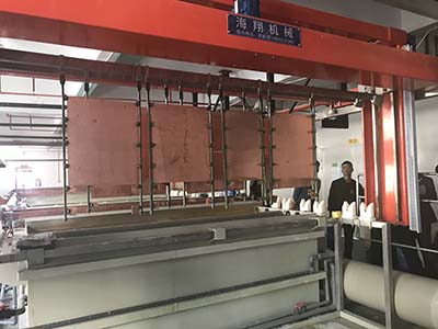
 Factory & Certificate


-

-
-
-

-
Nine standards for RF in PCB design
Nine standards for RF in PCB design,mainly use 4-6 layers.
5021 3 0 Shares
-

-
-
-
-
PCB process skills based on GENESIS2000 software (3)
7. Solder mask 8. BGA plug hole 9. Network comparison 10. Character layer
5318 2 0 Shares
-
PCB process skills based on GENESIS2000 software (2)
4. Drilling Editing 5. Drilling Outline Drawing 6. Circuit Layer
5177 1 0 Shares
-

-
-
-
-
-

-
-

-
Categories
Recommended Article:
- How Can AI PCB Design Software Streamline Manufacturing with NextPCB Templates?
- PCB Stackup for SMT Assembly: Thickness, Copper, Finish — What You Must Specify (and Why)
- PCB & PCBA in Smart Power Grid: Applications, Challenges & Technical Standards
- How to Prepare PCB Files for Assembly: Gerber, BOM, Stackup & More
- 2-Layer or 4-Layer PCB? Don't Let a Few Dollars Difference Ruin Your Circuit Prototype
- Arduino PCB Design Guide for Beginners
- The Ultimate Guide to Choosing Top Printed Circuit Board Manufacturers in 2026
- IoT Application and PCB/HDI Technical Challenges: From Smart Devices to Industrial Gateways
- Arduino Nano Pinout Diagram & Custom PCB Design Guide (2026)
- 4-Layer PCB Stackup Design and Impedance Control