High-speed digital and analog designs take circuit design to a whole new level, introducing complex electromagnetic behavior to the textbook flow-of-electrons analogy of electrical signals. One unavoidable challenge of high-speed PCB design is impedance control, or rather, impedance matching of high-speed signals to limit reflections, losses, and noise for the purpose of preserving signal integrity (SI). Tackling such challenges requires early collaboration from multiple parties in the product development process, from schematic designers, layout engineers, to the PCB fabricator.
NextPCB's PCB manufacturing capabilities extend beyond simple PCB manufacture. Specializing in reliable multilayer PCB manufacturing, NextPCB's impedance control services cater to signal integrity and applications requirements of all levels, providing you with the tools and flexibility to maximize high-speed performance. From impedance tuning and validation to advanced high-speed and high-frequency materials, turn to NextPCB for easy, cost-effective and repeatable impedance control.
Why is impedance control important in high-speed PCBs?
Impedance control is essential for maintaining the signal integrity of high-speed signals. Failure to reduce impedance mismatches can result in catastrophic performance or compliance failures, including timing skew, bit errors, packet loss, reduced power efficiency and long-term reliability issues.
As faster data rates and higher bandwidths become the standard in everyday electronics, effective high-speed design strategies have never been more important. Technologies like USB4, PCIe Gen 6, 5G, Wi-Fi 7, and mmWave radar will only put more pressure on high-speed and high-frequency product development, calling for close collaboration and meticulous planning across the entire product development team.
As a reliable multilayer PCB manufacturer, NextPCB understands the importance of client-manufacturer synergy and the role of the manufacturer in optimizing signal integrity and performance. Whatever your impedance control needs, from manufacturing capabilities and resources, to testing and validation, with NextPCB, you have support for various strategies, volumes and budgets.
How can NextPCB help you achieve your signal integrity goals?
Use NextPCB's stack-up selector and batch impedance calculator with our standard quickturn service for the most cost-effective impedance-controlled PCBs. Specify your topology from single-ended, differential pair and coplanar options and calculate the trace widths required with NextPCB's various standard stack-ups. NextPCB has over 40 different standard stack-ups for various board thicknesses available at no additional cost, including plain core and pseudo-8-layer boards calculated within 2Ω tolerance (actual manufactured tolerance ranges from 5-10%). Read More -> How to use Standard PCB Stackups for Controlled Impedance
Assisted Impedance Tuning and TDR Coupon Validation
Skip the hassle of calculations and tell our engineers your impedance control requirements. We'll tune the widths and create the stack-up for your design which we'll confirm with you before proceeding to manufacture. An impedance coupon will also be added to the production panel which replicates the exact geometry of the target traces. This will be used to non-destructively validate the impedance of the traces using TDR (Time Domain Reflectometry) measurements.
Microsection Analysis
Request a microsection report for detailed analysis of the PCB's internal structure, including dielectric and copper thicknesses and PTH/via integrity against IPC testing standards.

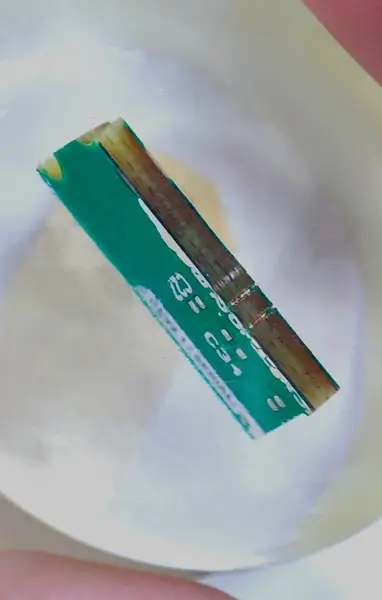
Microsectioned board sample used for analysis
Custom Stack-ups
NextPCB also supports custom stack-ups built to your specifications. This option is ideal for taking full control of your stack-up, for example, to replicate previously proven configurations that have been produced elsewhere.
NextPCB Standard PCB Impedance Control Capabilities
| Category |
Details |
| Stack-ups |
40+ standard stack-ups at no additional cost |
| Impedance Types |
| Single-ended: |
Up to 75 Ω |
| Differential: |
Up to 150 Ω |
|
| Tolerance: |
| > 50 Ω: |
± 10% |
| ≤ 50 Ω: |
± 5% |
|
Dielectric Constant
(reference value) |
| Core/Prepreg: |
4.2 |
| Solder mask: |
3.5 |
|
| Minimum Trace Width |
3 mil |
| Services |
- Impedance control tuning and TDR coupon validation
- Microsection Report
- Stack-up and impedance calculator
- Custom stack-ups
- Filled vias
|
Get an instant quote
Or inquire for more capabilities.
Advanced Capabilities
High-Speed and High-Frequency Dielectric Materials
Choose NextPCB's Advanced PCB service for a wide range of laminates from leading brands with low dielectric constants, loss tangents and stable dielectric loss at high frequencies. Choose from Isola, Nanya, TUC, Panasonic, ITEQ high-speed laminates, Rogers PTFE or non-PTFE high-frequency laminates, or inquire for more options.
Hybrid Stack-ups
Reducing the number of specialist laminates in a stack-up is a simple way of reducing material costs. However, specialist techniques and experience are required for building hybrid stack-ups containing laminates with different materials (e.g. Rogers RO4530B with standard FR4). NextPCB's experience with building hybrid PCBs can help you save costs without severely compromising build quality or performance.
Smooth Copper Foils
Copper roughness introduces frequency-dependent losses, degrading signal quality in high-speed designs through to the skin effect, phase distortion and localized impedance variations. If dielectric losses are already low, copper roughness becomes the dominant factor, contributing as much as 30% more losses compared to smooth copper. In addition to rolled-annealed (smooth copper) cladded laminates, NextPCB also supports smooth copper foil options, ensuring lower insertion loss in high-speed designs.
Ultra-fine copper geometries
Don't let manufacturing constraints become a limiting factor in your high-speed designs. NextPCB's advanced service's copper trace width capabilities go down to 2mils, essential for higher impedance values and dense routing.
Filled Vias and Via Backdrilling
Vias are major discontinuities in a signal's path, but avoiding them altogether is impractical. NextPCB supports PCB backdrilling and via filling techniques to remove via stubs and airgaps, thereby minimizing reflections and parasitic capacitance. Via fill and cap with non-conductive epoxy (VII) is also available via the standard PCB service.
Thermal Management Techniques
At higher speeds and frequencies, effective thermal management becomes an increasing issue. NextPCB supports heavy copper, embedded copper/copper coin technology and metal-core and ceramic materials for specialist applications.
> Recommend reading: PCB Thermal Design Basics (1): Substrate Material Selection
NextPCB Advanced PCB Impedance Control Capabilities
| Category |
Details |
| Stack-ups |
Custom and hybrid PCB stack-ups |
| Materials |
High-Speed PCB materials
Low-Dk and Low-Df laminates from major brands including Megatron and Isola, suitable for speeds from 1 to 56 Gbps. Learn more
High-Frequency materials
Ultra low-Dk and low-Df Rogers PTFE and non-PTFE laminates and ceramic PCBs. Learn more
|
| Minimum Trace Widths |
3 mil |
| Fabrication techniques |
- PCB backdrill
- LP/VLP/RA smooth copper foils
- Embedded copper/copper coin technology
- Filled vias
|
Get a quote
Or inquire for more advanced capabilities.
Why Choose NextPCB for your Impedance-Controlled PCBs?
Online Quotation Form and MES Integration
Make sure your impedance requirements are at the forefront and not just an afterthought. NextPCB's self-developed MES (manufacturing execution system) and online quotation form allow you to tailor your impedance control requirements and ensure every relevant production stage is prepared to build your boards to spec.
Engineering Expertise
Talk to engineers who understand your requirements and can offer suggestions to reduce manufacturing complexity and cost.
Repeatability Reassured
Our system allows you to repeat previous orders following the exact same parameters and requirements as the previous run, ensuring your impedance configurations are followed without having to go through the entire process again.
Choose NextPCB for maximum control and flexibility for your high-speed and high-frequency designs today. Get an online quotation or contact us for more information.

 NextPCB Capabilities
 PCB Assembly
 Layer Buildup
 SMD-Stencils
 PCB Design-Aid & Layout
 Mechanics
 Quality
 Drills & Throughplating
 Factory & Certificate
 PCB Assembly Factory Show
Certificate
PCB Assembly Factory Show
Certificate
 NextPCB Capabilities
 PCB Assembly
 Layer Buildup
 SMD-Stencils
 PCB Design-Aid & Layout
 Mechanics
 Surface
 Quality
 Drills & Throughplating
 Factory & Certificate


