
 NextPCB Capabilities
Printed Circuit Boards
NextPCB Capabilities
Printed Circuit Boards
 PCB Assembly
 Layer Buildup
 SMD-Stencils
 PCB Design-Aid & Layout
 Mechanics
 Quality
 Drills & Throughplating
 Factory & Certificate
 PCB Assembly Factory Show
Certificate
PCB Assembly Factory Show
Certificate
Support Team
Feedback:
support@nextpcb.com


For many hardware startups, makers, and students, transitioning from a 2-layer to a 4-layer PCB is a true rite of passage. You've moved past the limitations of simple boards because your designs now demand the precision of robust power distribution, signal integrity, and EMI control. Embracing a 4-layer stack-up is often the secret ingredient to unlocking high-speed data performance and taking your project from a fragile prototype to a reliable product.
However, the barrier to entry is rarely technical—it's economic. Many engineers hesitate, fearing that 'cheap' necessarily means 'unreliable.' But this is a misconception; the real goal isn't to find the cheapest board, but to find the highest value—a balance of performance, reliability, and manufacturing cost. You need an affordable 4-layer solution that won't fail during assembly or turn into an EMI nightmare in your final product.
When you make the right design and manufacturing decisions, you'll find that a well-engineered 4-layer board provides the stability you need, all while remaining surprisingly accessible.
This guide will show you how to engineer your project for high performance on a budget. No fluff —just what works.
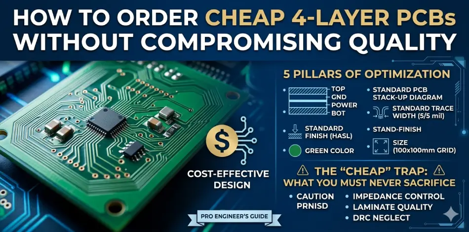
A standard 4-layer PCB consists of four copper layers separated by insulating material (prepreg and core). A typical professional stack-up looks like this:
| Layer | Function | Benefit |
|---|---|---|
| Top Layer | Component placement & signal routing | Easy access |
| Inner Layer 1 | Ground plane | EMI shielding, return path |
| Inner Layer 2 | Power plane | Clean power distribution |
| Bottom Layer | Signal routing & components | Extra routing space |
Many engineers start with 2 layers pcb because it's cheaper upfront. But as circuit complexity increases, 2-layer designs create problems:
A 4 layer PCB often reduces engineering time because designers get dedicated power and ground layers. Compared with a 2-layer board, a 4-layer board gives you:
Skipping these benefits is false economy. A 4-layer board is a long-term investment in your project's stability.
The bottom line: A cheap 4 layer PCB is not always the cheapest solution if it increases your development costs later.
You don't need a massive budget to get professional-grade boards. You need to Design for Manufacturing (DFM). Here is how to keep your 4-layer PCB costs in the "prototype" bracket.
Complexity costs money. Manufacturers offer lower prices for "standard" specifications because they can batch your board with hundreds of others.
| Feature | Expensive (Hard) | Affordable (Standard) |
|---|---|---|
| Trace/Space | 3 mil / 3 mil | 5 mil / 5 mil or 6 mil / 6 mil |
| Minimum via hole | 0.15 mm (6 mil) | 0.3 mm (12 mil) or larger |
| Via type | Blind, buried, or micro vias | Standard through-hole vias only |
Pushing to 3/3 mil or using micro-vias often triggers a price jump. Stick to standard specs whenever your design allows.
> Recommend reading: Blind Vias and Buried Vias: What Is the Difference in PCB?
Surface Finish: Opt for Lead-Free HASL (Hot Air Solder Leveling). It is the most robust and cost-effective surface finish for most applications. Only choose ENIG (Immersion Gold) if you are working with fine-pitch BGA components (0.4mm pitch or smaller).
Solder Mask Color: Keep it green. Standard green solder mask is produced in massive, optimized volumes. Choosing matte black, white, or blue require stopping the line, cleaning tanks, and running a special batch. That adds 10-20% cost and lead time.
Material: Unless you are working with high-frequency RF or extreme temperatures, standard FR-4 (Tg 130-140°C) is perfectly adequate.
| Material | Cost | Typical Use |
|---|---|---|
| Standard FR-4 (Tg 130-140) | Low | General electronics, IoT, prototypes |
| High-Tg FR-4 (170+) | Medium | Industrial, high-temp environments |
| Rogers / RF materials | High | RF, microwave designs |
> Recommend reading: PCB Surface Finishing 101: Processes, Pros & Cons
Most manufacturers have a "sweet spot" for pricing. Check if your board fits within standard dimensions like 10x10mm, 30x30mm or 100x100mm.
Reducing your footprint by even 5mm could move your design from a higher pricing bracket to a lower one. A 100x100mm board costs significantly less than a 120x120mm board because more boards fit on a standard manufacturing panel.
In the PCB industry, the "smaller-is-more-expensive" phenomenon occurs because the fixed overhead costs for engineering and automated processing, combined with poor panel utilization rates, complex work-holding requirements, and higher handling/scrap risks associated with micro-sized boards, are disproportionately amortized over a smaller surface area, resulting in significantly higher unit costs compared to standard-sized panels.
If you have multiple small designs, don't order them individually. Combine them into a single panel using V-scoring or tab routing.
Many prototype shops allow "tiling"—sharing the fixed setup costs across multiple designs. You can get five different boards for the price of one panel.
> Recommend reading: NextPCB Multi-Design Ordering Specification: Different PCB Designs in Gerber Files
Tenting vias (covering them with solder mask) is good for reliability, but if you don't need it, don't pay extra for the processing.
Always check if "via tenting" is a free standard feature or a paid add-on at your chosen shop. Many fabs include it by default; some charge extra.
> Recommend reading: Custom PCB and PCBA Cost Analysis: How to Optimize Design and Reduce Expenses
Not all "cheap" is good. Here's where to save versus where to spend a little more.
| Feature | Save Money (Cheap) | Spend a Little (Value) | Why? |
|---|---|---|---|
| Material | Unknown brand FR-4 | Known brand (KB, ITEQ, ShengYi) | No-name materials can delaminate during soldering. |
| Hole size | 0.2 mm (8 mil) | 0.3 mm (12 mil) | Fewer drill breakages = lower risk of scrapped boards. |
| Copper weight | 1 oz internal & external | 0.5 oz internal, 1 oz external | Signals don't need 1 oz. Saves etching cost. |
| Soldermask | Green | Green | No reason to pay extra for blue. |
| Electrical test | None (trust the fab) | 100% Flying probe | Never skip this. A single open via kills your week. |
The golden rule: Pay for 100% electrical testing and a reputable FR-4 brand. Save money on color, exotic finishes, and ultra-fine tolerances.
See How Your Boards Inspected By NextPCB
A. IoT Prototyper (ESP32, Wi-Fi, BLE)
Problem: 2-layer board has noise issues, Wi-Fi range is poor.
4-layer strategy: Top (Signal) → Inner 1 (GND) → Inner 2 (Power) → Bottom (Signal). Noise disappears for an extra $20. Worth every penny.
B. Hardware Startup (Pre-seed, 20 beta units)
Problem: Need multiple circuit blocks tested.
4-layer strategy: Combine 5 different designs into one "mother panel." V-score it. You get 20 boards for the price of 4 panels.
C. DIY Synthesizer / Audio
Problem: 50 Hz hum from power supply.
4-layer strategy: Dedicate Inner 2 layer to +12V and -12V planes. Clean audio, no hum.
Reducing cost does not mean removing critical specifications.
If you are running high-speed signals (USB, Ethernet, PCIe, DDR memory), you must specify impedance requirements. A cheap board without controlled impedance is just an expensive coaster.
The fix: Most online fabs publish "standard impedance stack-ups" for 4-layer boards. Ask for their 50Ω single-ended or 90Ω differential pair calculator. It's usually free.
PCB Impedance Calculator Online
Always ensure your supplier uses certified FR-4 from known brands (KB, ITEQ, ShengYi, etc.). "Mystery" laminate materials can delaminate during reflow soldering, destroying your components and wasting your time.
Some very low-cost suppliers skip electrical testing to save $10-15 per order. The risk? You receive boards with broken vias or shorts. You waste hours debugging.
Never skip 100% electrical testing (flying probe or fixture). It is the cheapest insurance you can buy. NextPCB performs 100% Electrical Testing on every single board.
Many cheap board houses will reject or upcharge your order if your design files violate their basic DRC. Always run the Design Rule Check in your EDA software (KiCad, Altium, Eagle, or whatever you use) against the manufacturer's specs before submitting.
Get Your Designs Checked by HQDFM for Free
Before you upload your Gerber files, run through this list to save time and money.
Not every project needs the same level of specs. Match your choices to your project phase.
| Project Phase | Focus | Recommended Choices |
|---|---|---|
| Proof of Concept | Lowest cost | Green solder mask, HASL, 6/6 mil trace/space, standard FR-4 |
| Client/Demo Prototype | Balance | ENIG (if budget allows), green, 5/5 mil, clean silkscreen |
| Small Batch Production | Quality / Reliability | Impedance control (if needed), checked vias, High-Tg FR-4 for thermal demands |
Q: What is the typical price for a cheap 4-layer PCB prototype?
A: For a 50x50mm board, 5 pieces, standard FR-4, HASL, 1-week lead time: roughly $25–$50 USD from major Chinese fabs (JLCPCB, PCBWay, Seeed). US or EU fabs may charge $100–150 for the same.
Q: Is a cheap 4-layer PCB reliable for production (1000+ units)?
A: Yes, if you choose a verified manufacturer. Order a prototype run first. For mass production, negotiate "standard panel" pricing. Reliability comes from process control, not the price tag.
Q: How fast can I get a cheap 4-layer board?
A: "Cheap" usually means 5–7 business days for fabrication plus shipping. 24-hour turnaround costs 3–5x more. Plan your prototyping schedule accordingly.
Q: Does the number of vias affect price?
A: Slightly. A board with 500 vias costs roughly the same as one with 50 vias, unless you use plugged or tented vias as a paid add-on. Standard un-tented through-hole vias are usually included in base pricing.
Q: Is a 4-layer board always better than a 2-layer board?
A: For simple circuits with low speeds, a 2-layer board is fine. For complex designs requiring better routing, power management, and signal integrity, a 4-layer board is usually the better choice.
Q: Can I get controlled impedance on a cheap 4 layer PCB?
A: Yes. Most online fabs publish "standard impedance stack-ups" for 4 layers. Ask for their 50Ω single-ended or 90Ω differential pair calculator. It's usually free.
Let's be clear:
| Cheap PCB Choice | Cost-Effective Choice |
|---|---|
| Lowest price only | Balanced price + reliability |
| Unknown material | Standard FR-4 from known brand |
| No DFM review | Free design rule check included |
| Skipped electrical test | 100% flying probe |
| Extreme specs (3/3 mil) | Standard rules (5/5 mil) |
| Risk of failure | Stable, predictable quality |
The goal of choosing a "cheap 4 layer PCB" should not be finding the lowest possible price.
The smarter approach is optimizing:
Design + Materials + Manufacturing Process + Supplier Capability
A properly optimized 4 layer PCB delivers professional performance while keeping manufacturing costs under control.
For engineers, startups, and hardware developers, the best PCB solution is not the cheapest board — it is the board that provides the highest value for your budget.
Ready to start your next design? Check our 4-Layer PCB Design & Cost Optimization Checklist to make sure your next project is optimized for both performance and your wallet.
Still, need help? Contact Us: support@nextpcb.com
Need a PCB or PCBA quote? Quote now


 Surface

