
 NextPCB Capabilities
Printed Circuit Boards
NextPCB Capabilities
Printed Circuit Boards
 PCB Assembly
 Layer Buildup
 SMD-Stencils
 PCB Design-Aid & Layout
 Mechanics
 Quality
 Drills & Throughplating
 Factory & Certificate
 PCB Assembly Factory Show
Certificate
PCB Assembly Factory Show
Certificate
Support Team
Feedback:
support@nextpcb.com


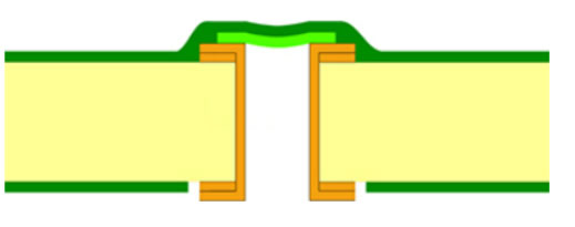
Vias are an essential component of PCB, serving as the connection pathways between the board'sboard's layer. The holes, often copper-plated, play a crucial role in ensuring that the PCB functions as intended. Manufacturers use two standard methods to cover these vias: masked or filled via, where the hole is fully covered, and tenting, where the hole is barely covered. Tenting is a popular method among PCB designers as it allows the vias to conduct electrical signals and dissipate heat.
Tenting via refers to a process in printed circuit board (PCB) manufacturing. The metal or resin filled the unused vias on PCB. It protects them from contamination and electrical shorts. Vias are small cylindrical or conical holes drilled through the layers of a PCB. It allows electrical signals to pass between the top and bottom of the board. In some cases, not all vias are required for electrical connections. And these unused vias can cause electrical problems if left uncovered. Tenting helps address these issues by filling the unused vias, making the PCB more reliable and durable.
It can also improve the appearance of the PCB, as the filled vias blend in with the surface of the board and do not detract from its overall appearance. This can be especially important in applications where the appearance of the PCB is a consideration.
In addition to its benefits for reliability and appearance, it can also make the PCB more durable. The filled vias provide additional structural support to the board. It makes it less likely to suffer from damage during handling or assembly. This can be particularly important in applications where the PCB will be subject to high levels of stress or vibration, such as in aerospace or military systems.
Moreover, tenting via is a valuable process in PCB manufacturing that can improve the finished product's reliability, performance, and appearance.
Tenting vias may not be the optimal approach for via coverage due to certain drawbacks. One disadvantage is that the liquid solder masks used in tenting can potentially cause the LPI to break. It results in small holes in the tent that may trap moisture and chemicals, leading to corrosion and damage to the PCB.
During the prototype stage of PCB production, leaving the vias uncovered can aid in identifying any trace issues, enabling prompt resolution and re-routing. Masking the vias could impede the detection and resolution of these problems before they become irreversible.
This process can vary depending on the type of via being filled and the specific requirements of the PCB application. But the basic steps include the same filling, curing, and finishing of the vias. The tenting process can be performed manually or by using automated equipment. It depends on the volume of PCBs being manufactured and the application's specific requirements.
There are some factors that determine if you need the tented vias or not. The first factor is the PCB design, and the second factor is the size of the via. Tenting works better with the vias having smaller dimeters of 12 mils. Whereas tenting didn't work well with the via that is 12 mil in diameter. For the larger vias, it is better to have some kind of fill to close it.
Besides, if you are looking for a cost-effective option, you can work with this tenting as it provides a better option compared to mask plugging or epoxy filling. The best and the most cost-effective option in this tenting includes a liquid photo-imageable solder mask. While if you are seeking the loose tenting option, the epoxy filling is the best choice, although it is quite expensive.
Furthermore, tenting prevents exposure to environmental factors reducing device lifetime like humidity and chemicals.
Tented Via is one of the most common practices to protect the PCB board. Because of the cost factor, it is often chosen over mask plugging or epoxy filling.
If the copper elements and the holes in PCBs are left exposed, then the outside elements can corrode and damage the PCB. Thus, it helps to improve the reliability of the circuit. It also reduces electromagnetic interference (EMI) by providing physical barriers between the signal layers on PCB. Thus, the performance of the PCB can be improved by improving the reliability and reducing the EMI.
Tenting via is an essential process in PCB manufacturing that can help to improve the reliability, performance, and aesthetics of the finished PCB. By implementing tenting via, manufacturers can ensure that their PCBs meet modern electronic applications' rigorous demands.
The via is covered with a stretched Dry film solder mask without any additional materials.
One-Sided: Type I-a

Double-Sided: Type I-b
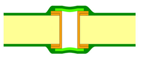
The entire via has been coated with a layer of dry film solder mask. Then a layer of regular solder mask was printed on top of it.
One-Sided: Type II-a
Double-Sided: type II-b
Tenting Via is a critical aspect of printed circuit board (PCB) manufacturing. Choose the best manufacturer for all of your PCB services.
NextPCB can transform your ideas into reality with our professional PCB services. We provide an easy way to check the vias in your required designs. Trust us to bring your designs to life with precision and expertise. Contact us today to learn more about how we can help you bring your project to the next level.
Still, need help? Contact Us: support@nextpcb.com
Need a PCB or PCBA quote? Quote now


 Surface

