

 Surface


Julia Wu - Senior Sales Engineer at NextPCB.com

 NextPCB Capabilities
Printed Circuit Boards
NextPCB Capabilities
Printed Circuit Boards
 PCB Assembly
 Layer Buildup
 SMD-Stencils
 PCB Design-Aid & Layout
 Mechanics
 Quality
 Drills & Throughplating
 Factory & Certificate
 PCB Assembly Factory Show
Certificate
PCB Assembly Factory Show
Certificate

Support Team
Feedback:
support@nextpcb.com


A through-glass via (TGV) is a vertical conductive via formed through a glass substrate or glass interposer, used to electrically connect the two sides of the glass or link stacked layers — functionally similar to the through-silicon via (TSV) used in silicon-based packaging. TGV is one of the key process bottlenecks determining whether glass substrate technology can scale, since via precision, aspect ratio, and metallization quality directly determine interconnect density and reliability.
Glass itself is an insulator. To achieve multi-layer routing interconnects on a glass core substrate or glass interposer, vias must first be formed through the glass, then metallized (typically with copper fill) to form a conductive path. The precision and yield of TGV processing largely determine whether glass substrates can match or exceed the interconnect density of organic substrates or silicon interposers. This is one of the most closely watched process bottlenecks in the glass substrate technology chain.
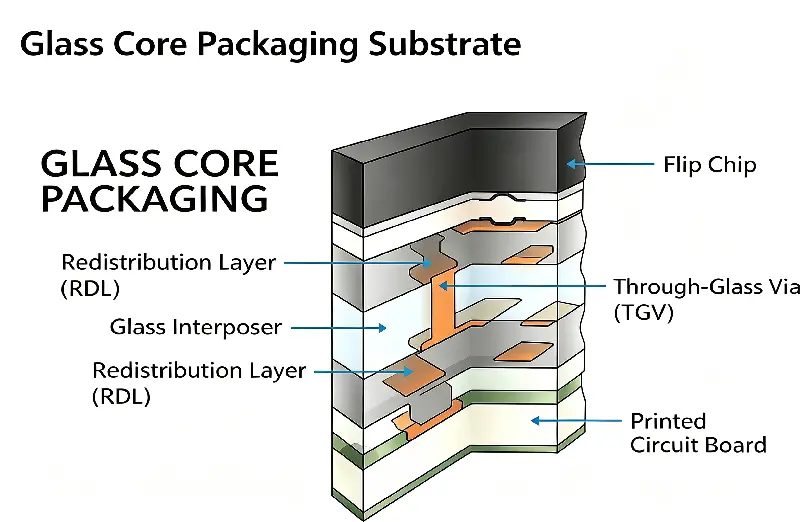
In conventional PCB manufacturing, microvias are typically formed by mechanical drilling or CO2 laser ablation of organic material — a mature, well-understood process. But glass has a fundamentally different mechanical behavior from organic laminate or copper foil: glass has essentially no plastic deformation capacity. Under mechanical stress, it doesn't bend and yield the way organic material does — it fractures brittlely along a crack propagation path. This means that once a mechanical drill bit contacts glass, cracks can easily propagate unpredictably through the substrate rather than staying confined to the intended via location, often scrapping the entire panel rather than failing just one via. This is why TGV processing must rely on non-contact laser-based approaches rather than simply reusing the mechanical drilling or punching equipment the PCB industry has already perfected — glass substrates and PCBs may look like the same "drill-then-plate" logic on the surface, but the material failure modes are entirely different, and process inheritance between the two is actually quite limited.
| Dimension | TSV (Through-Silicon Via) | TGV (Through-Glass Via) |
|---|---|---|
| Base material | Silicon | Glass |
| Processing method | Primarily deep reactive-ion etching (DRIE) | Laser-induced etching, direct laser ablation, photosensitive glass — multiple approaches coexist |
| Material cost | Relatively higher | Raw glass cost is relatively lower, but the process is still maturing |
| Electrical / optical properties | Semiconductor behavior, requires additional insulation layers | Naturally insulating and transparent, lower parasitic capacitance |
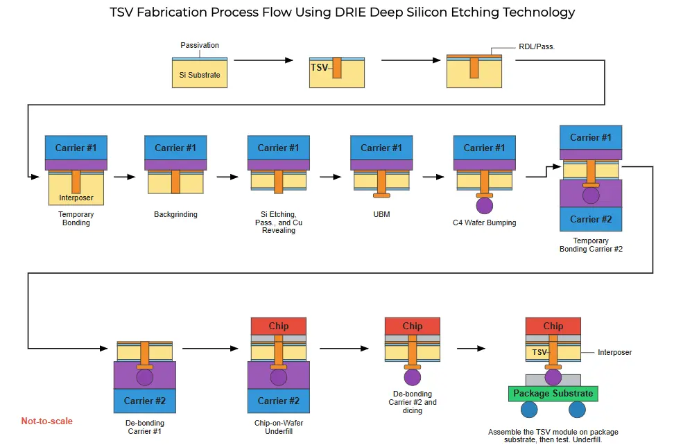
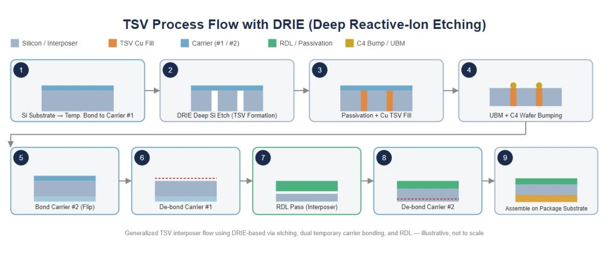
Process flow diagram of through-silicon via (TSV) fabrication using deep reactive-ion etching (DRIE)
Three main TGV processing approaches are currently being explored in the industry, each with its own trade-offs, and none has emerged as the dominant path yet:
The core TGV process metrics are via diameter, aspect ratio, and metallization yield. Public industry sources indicate aspect ratios in the range of 15:1 have been demonstrated, with via diameters achievable down to the micron scale. A higher aspect ratio means higher-density vertical interconnects can be achieved on thinner glass substrates, but it also raises the bar for metallization fill uniformity.
One of glass substrate's major selling points is that it can be processed at panel sizes far larger than a traditional 300mm silicon wafer (e.g., 500mm-class), theoretically lowering the per-unit-area interconnect cost. But this logic carries a hidden assumption: the defect density per unit area must stay constant — or ideally decrease. Under the yield models common in the semiconductor industry, the probability that a substrate contains at least one fatal defect rises as area increases. If TGV process defect rates (voids, micro-cracks, uncontrolled taper) don't fall in step with growing panel size, panel-level packaging won't automatically deliver a cost advantage — it may instead amplify cost volatility, since scrapped area is larger and each scrap event is more costly. This is why TGV yield improvement tends to draw more industry attention than simply "can we drill this via at all" — what really determines the pace of commercialization is whether defect density can keep up with the rate of panel-size expansion.
They serve a similar function — both provide vertical interconnects — but the base material and processing methods are completely different. In the near term, they're more likely to develop in parallel depending on the application, rather than replace one another.
TGV remains in process-route validation and small-scale pilot production. The three main processing methods (laser-induced etching, direct laser ablation, photosensitive glass) have not yet converged on a single industry-standard path.
Via-wall micro-crack control and metallization fill uniformity in high-aspect-ratio vias are the two bottlenecks most frequently cited in public technical sources.
Taper refers to the hourglass-shaped via cross-section that narrows slightly toward the middle, caused primarily by the isotropic diffusion nature of wet chemical etching — etchant near the via opening has longer contact time and a higher removal rate. Taper control is a key indicator of how mature a given laser-etch process is, since it directly affects downstream metallization uniformity.
Because glass has essentially no plastic deformation capacity, mechanical stress causes cracks to propagate unpredictably through the substrate rather than staying confined to the intended via location, often scrapping the entire panel. This is why TGV must rely on a non-contact laser-modification-plus-etch process instead.
NextPCB provides precision drilling and plating capabilities for high-density interconnect (HDI) microvias and blind/buried vias. If your project involves these capabilities, explore NextPCB's HDI PCB manufacturing capabilities.

Still, need help? Contact Us: support@nextpcb.com
Need a PCB or PCBA quote? Quote now

