NextPCB Capabilities
 PCB Assembly
 Layer Buildup
 SMD-Stencils
 PCB Design-Aid & Layout
 Mechanics
 Surface
 Quality
 Drills & Throughplating
 Factory & Certificate





Glass Substrate Supply Chain and Key Players: Who's Doing What
Most coverage of glass substrate progress focuses on a handful of headline names — Intel, Samsung, a Korean subsidiary or two — and treats "glass substrate is coming" as a single, undifferentiated story. In reality, the supply chain has at least six distinct layers, each with its own set of leading players and its own technical bottleneck, and the companies furthest from the spotlight — equipment and specialty-chemistry suppliers — may end up mattering more to the commercialization timeline than the chipmakers whose names actually make headlines.
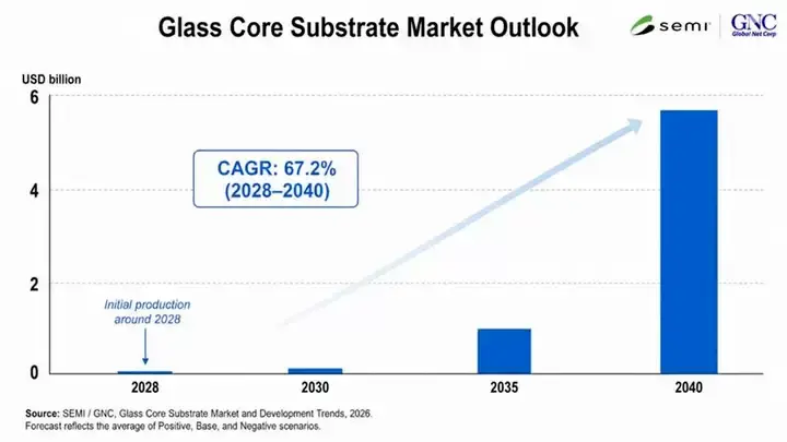
Glass Core Substrate Market Outlook
The Glass Substrate Value Chain: Six Layers
| Layer | Function | Key Players |
|---|---|---|
| Glass materials | Low-CTE, low-dielectric-loss glass compositions | Corning, AGC, SCHOTT, Nippon Electric Glass (NEG) |
| TGV equipment | Laser-based via formation tooling | LPKF, Philoptics |
| Plating & etch materials/equipment | Metallization chemistry and process tools | Lam Research, YCChem, Soulbrain |
| Substrate manufacturing & assembly | Panel processing, RDL build-up | Absolics (SKC), Samsung Electro-Mechanics, LG Innotek |
| Inspection & metrology | Panel-scale defect detection | Applied Materials, Onto Innovation, KLA, Camtek |
| End customers / integration | Chip design and packaging integration | Intel, AMD, NVIDIA, TSMC, hyperscalers (e.g. AWS) |
Every layer of this chain ultimately comes down to the same underlying requirement as conventional PCB manufacturing at a smaller scale: holding precise tolerances on fine routing and via formation, repeatably, at volume. If your own project needs that kind of precision today rather than on a multi-year glass substrate roadmap, explore NextPCB's HDI PCB manufacturing capabilities.
Two Strategic Models: Vertical Integration vs. Merchant Supply
The three most-cited players — Intel, Absolics, and Samsung — are pursuing meaningfully different strategies, and the difference matters for anyone trying to read their announcements correctly.
Intel has taken a vertical-integration approach, reportedly investing more than $1 billion into its glass substrate pilot line in Chandler, Arizona, and by early 2026 was producing glass cores tied to its 18A and 14A process nodes in-house. In January 2026, Intel showed a sample combining its EMIB (Embedded Multi-die Interconnect Bridge) packaging with a glass core substrate at NEPCON Japan, reportedly reaching a "no micro-crack" milestone in the process — and demonstrating a package built to roughly 78×77mm supporting around 1,716mm² of silicon, an area that exceeds a single silicon reticle field (source). Controlling substrate production in-house fits Intel's broader foundry strategy: it lets Intel offer differentiated yield and integration to hyperscale customers designing custom AI silicon, rather than depending on an external merchant supplier's roadmap.
Absolics, a subsidiary of Korea's SKC and backed in part by Applied Materials, has instead positioned itself as an open-market merchant supplier — building substrates for whichever customer wants them, rather than exclusively for internal use. Its roughly $600 million facility in Covington, Georgia has been reported as ramping toward 20,000 sheets per month, and Absolics has entered the certification stage with customers including AMD (reportedly tied to AMD's Instinct MI400 series) and AWS (source). Absolics has also reportedly pursued a dual-track technical strategy — an "embedding" approach aimed at high-end AI data center performance, alongside a faster-to-commercialize "non-embedding" approach — reflecting a merchant supplier's need to serve both premium and speed-to-market customer segments simultaneously, rather than optimizing for a single internal roadmap the way Intel can.
Samsung has taken a third approach: a cross-division "Triple Alliance" strategy coordinating its electronics, display, and electro-mechanics units, leveraging glass-handling expertise the group already has from its display business. Samsung has reportedly readied a high-volume pilot line in Sejong, South Korea, and is exploring glass core substrates as an option alongside its existing I-Cube and H-Cube 2.5D packaging offerings (source).
The Real Bottleneck Isn't the Glass — It's the Equipment Layer
Raw low-CTE glass itself is a well-understood, decades-old material category; Corning, AGC, SCHOTT, and NEG aren't solving a materials-science mystery so much as adapting existing glass compositions to a new application. The harder, less visible bottleneck sits one layer down, in TGV processing equipment and plating chemistry — which is consistent with the metallization yield and void-formation challenges discussed in our companion article on through-glass via (TGV) technology. Equipment suppliers like LPKF and Philoptics effectively set the ceiling on what yield any substrate manufacturer can achieve, regardless of how good their glass is (source). Specialty plating-chemistry suppliers occupy a particularly interesting position in this chain: additive formulations designed specifically to prevent voids during high-aspect-ratio copper fill function as a recurring consumable, tied directly to production volume rather than a one-time equipment sale — meaning their commercial fortunes are more closely tied to actual production ramp than to announcement cycles or pilot-line headlines.
China's Entry: BOE and the Broader Landscape
Outside the US-Korea-Japan axis that dominates most coverage, Chinese display maker BOE has reportedly been running a pilot glass substrate production line and has made progress on TGV technology, with some reports suggesting mass production plans as early as this year (source). Given how early-stage and fast-moving this space is, and how much incentive companies have to announce ambitious timelines publicly, any single-source production date — including this one — should be treated as directional rather than confirmed until corroborated elsewhere.
Timeline: Whose Roadmap Is Realistic?
Published timelines from different sources don't fully agree with each other, which is itself informative. Some reporting describes Absolics targeting a form of commercial-scale production by the end of 2026 (source); other coverage describes Intel's own production window in broader terms, such as "the second half of this decade"; and TSMC has reportedly been preparing a glass-panel (CoPoS) pilot line targeting completion around mid-2026, partly to support NVIDIA's upcoming "Rubin" generation of GPUs. Independent market-research coverage of the broader category is available from firms such as IDTechEx and Future Markets Inc, for readers who want a more detailed forecast breakdown. The spread between these estimates is a useful reminder that "glass substrate mass production" isn't one single milestone the whole industry crosses at once — different companies, different product types (core substrate vs. interposer), and different customer certification requirements will each hit commercial volume on their own schedule.
Frequently Asked Questions
Who is currently leading glass substrate commercialization?
Intel, Absolics (SKC), and Samsung are the most frequently cited leaders, but they're pursuing different strategic models — vertical integration, merchant supply, and cross-division alliance, respectively — so "leading" depends on which metric (investment, in-house yield, open-market availability) you're measuring.
Can I already buy glass substrates from a merchant supplier?
As of mid-2026, merchant supply is still in customer certification stages with select partners (such as Absolics' reported work with AMD and AWS) rather than broadly available for general purchase.
What's actually holding back glass substrate scale-up?
Industry analysis points to TGV processing equipment yield and plating chemistry as the tighter bottleneck, more so than the underlying glass material itself, which is a comparatively mature material category.
Is glass substrate development happening outside the US, Korea, and Japan?
Yes — Chinese display maker BOE has reportedly been developing pilot-scale glass substrate and TGV capability, though specific production timelines from this and other regions should be treated cautiously until corroborated by multiple independent sources.
When will glass substrate reach mass production?
There isn't a single agreed-upon date. Different companies and product types (core substrate vs. interposer) are on different timelines, with some targeting commercial milestones as early as late 2026 and others describing a multi-year runway extending toward the end of the decade.
While the glass substrate supply chain continues to mature, NextPCB can help you move forward today with production-ready PCB manufacturing for your current designs. Get an instant PCB quote to see pricing and lead time for your project.