NextPCB Capabilities
 PCB Assembly
 Layer Buildup
 SMD-Stencils
 PCB Design-Aid & Layout
 Mechanics
 Surface
 Quality
 Drills & Throughplating
 Factory & Certificate





Glass Core Substrate vs. Glass Interposer: What's the Actual Difference?
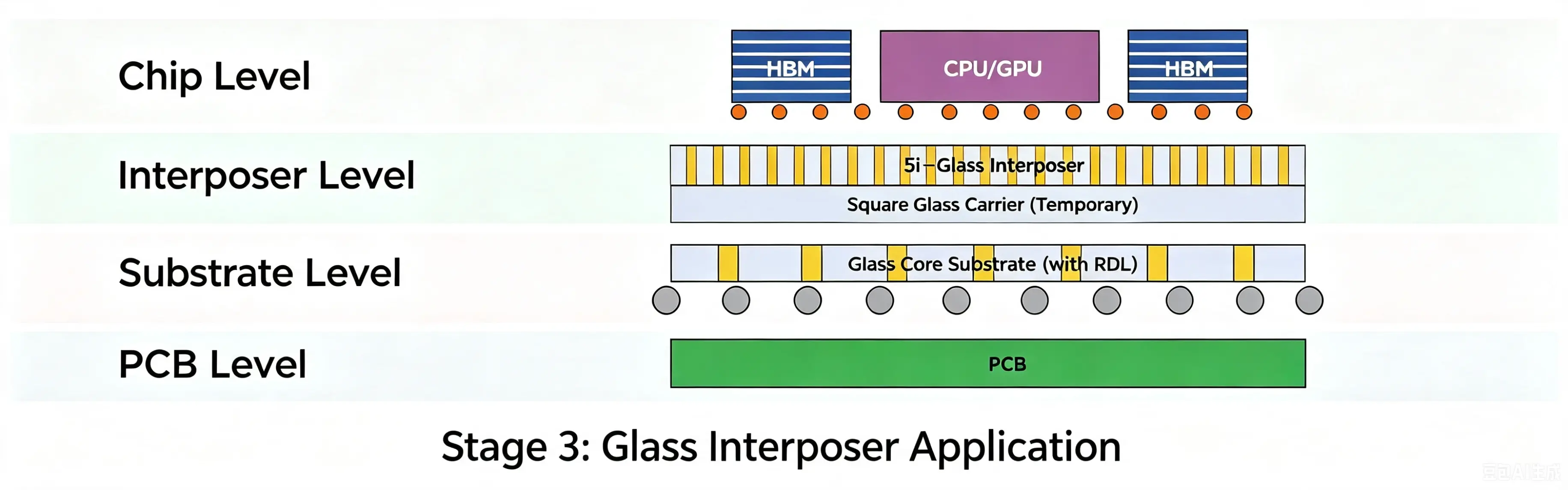
"Glass core substrate" and "glass interposer" are often used loosely — sometimes interchangeably — in marketing materials and even in some technical write-ups, but they refer to two different positions in the packaging stack, solving two different engineering problems. A glass core substrate replaces the organic core layer of a standard chip package substrate. A glass interposer replaces the silicon interposer that sits directly beneath the die stack. Confusing the two makes it hard to reason about which commercialization timeline, which process requirements, and which supplier ecosystem actually applies to a given claim you read about "glass substrate" progress.
Glass Core Substrate: Replacing the Organic Core Layer
In a conventional flip-chip package, the substrate sits between the die and the PCB, built up from a core layer (commonly BT resin or similar) with redistribution and buildup layers on both sides. A glass core substrate replaces that organic core with a glass panel, while the overall substrate architecture — die on top, multiple buildup/RDL layers, external bumps toward the PCB on the bottom — stays conceptually the same as what substrate suppliers already produce today. The main goal here is warpage control and dimensional stability at large substrate sizes, not necessarily ultra-fine interconnect pitch matching the die bump pitch directly.
Glass Interposer: Replacing the Silicon Interposer
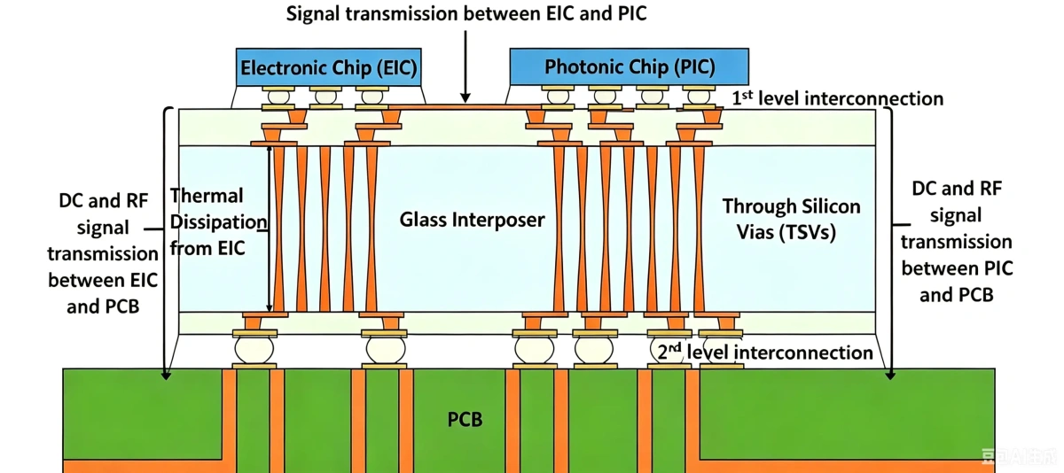
A glass interposer sits in a different position in the stack: directly underneath the die (or multiple dies — for example a GPU alongside HBM stacks), functioning as a high-density redistribution layer that fans out the die's extremely fine bump pitch before routing down to the coarser pitch of the package substrate below it. This is the same role a silicon interposer plays in a conventional CoWoS-style architecture, just executed in glass instead of silicon. Because it sits closer to the die, a glass interposer typically needs finer RDL pitch and higher TGV density per unit area than a glass core substrate does.
Architectural Comparison
| Dimension | Glass Core Substrate | Glass Interposer |
|---|---|---|
| Position in the stack | Package substrate core layer, between die and PCB | Directly beneath the die/HBM stack, between die and package substrate |
| Primary function | Warpage control, dimensional stability at large panel sizes | Ultra-fine-pitch fan-out redistribution between die and substrate |
| RDL pitch requirement | Relatively coarser, closer to existing substrate RDL norms | Much finer, closer to die-side bump pitch |
| TGV density requirement | Lower density per unit area | Higher density per unit area |
| Associated packaging schemes | Panel-level substrate approaches (e.g., CoPoS-style panel substrates) | Interposer-replacement approaches analogous to CoWoS-S, but glass-based |
| Commercialization timeline | Generally expected to reach volume production earlier | Generally expected to require a longer maturation runway |
These architectural differences aren't just conceptual — they translate into measurable, quantifiable gaps once you compare actual packaging schemes head-to-head. The table below breaks down how the traditional CoWoS silicon-interposer route stacks up against the emerging CoPoS glass-panel route on material efficiency, cost, and signal performance.
| Comparison Dimension | CoWoS (Traditional Route) | CoPoS (New Route) |
|---|---|---|
| Substrate Material | Silicon Interposer (Circular Wafer) | Glass Panel (Rectangular Panel) |
| Substrate Shape | Circular (300mm Wafer) | Rectangular (e.g., 510x515mm) |
| Material Utilization Rate | Approx. 70% (Edge Waste) | >95% (Square Panel Perfectly Matches Square Chips) |
| CTE Matching | Matches Silicon Chips, but Differs from Substrate | Highly Matches Silicon Chips, Greatly Reduces Warpage |
| Signal Loss | Good | Better (Glass is a High-Quality Insulator with Extremely Low High-Frequency Loss) |
| Packaging Cost | High (Silicon Interposer is Expensive) | Expected to Reduce by 20-30% |
| Interconnection Density | High | Higher (Glass Surface is Flat, Enabling Finer Lines) |
Both approaches ultimately depend on the same underlying capability: holding tight tolerances on fine-pitch routing and precision via formation at scale, whether the base material is glass, silicon, or organic laminate. If your project involves high-density interconnect (HDI) requirements — fine-pitch routing, blind/buried vias, or tight registration across build-up layers — explore NextPCB's HDI PCB manufacturing capabilities to see how these precision requirements translate into production-ready PCB manufacturing today.
Why the Two Terms Keep Getting Conflated
Part of the confusion is legitimate: both approaches use the same base material (glass) and often the same core enabling process (TGV), and both are frequently cited together in the same "glass substrate is coming" narrative. Industry announcements don't always specify which layer of the stack they're actually talking about, and a single supplier may be developing both a core-substrate product and an interposer product under overlapping branding. But treating them as one undifferentiated technology obscures a real difference in difficulty: an interposer sits closer to the die, so it inherits tighter tolerance requirements from the die's own bump pitch, while a core substrate has more room to interface with the coarser pitch already used on the PCB side.
Why Interposer-Level Glass Is the Harder Engineering Problem
Because a glass interposer must fan out from die-level bump pitch, its RDL lines and TGV pitch need to approach dimensions much closer to what silicon-based back-end-of-line processes achieve — a significantly tighter target than what a core substrate's buildup layers need to hit. Every process challenge already discussed for TGV — taper control, metallization void formation, panel-level defect density — gets harder as the required pitch shrinks and via density rises, because the tolerance for any single defect shrinks along with it. A core substrate, by contrast, can tolerate a coarser process window because it isn't trying to match die-level pitch directly; it only needs to bridge from the substrate's own RDL to the PCB-facing bumps below. This is the underlying reason glass core substrate is generally expected to reach commercial volume ahead of glass interposer, even though both rely on the same base material and the same TGV toolkit.
Which Comes First: A Commercialization Timeline View
Given the difficulty gap above, it's reasonable to expect glass core substrate to reach meaningful production volume before glass interposer does — the looser pitch tolerance lets it leverage panel-level infrastructure that's closer to being production-ready today. Glass interposer, by needing die-level pitch matching, effectively needs to close more of the gap with mature silicon back-end processes before it can scale, which typically means a longer runway. Readers evaluating supplier claims or roadmap announcements should check explicitly which of the two a given announcement is actually describing, rather than assuming "glass substrate progress" applies uniformly to both.
Frequently Asked Questions
Is a glass interposer the same as a glass core substrate?
No. A glass core substrate replaces the organic core layer of a package substrate, positioned between the die and the PCB. A glass interposer replaces the silicon interposer, positioned directly beneath the die stack, and typically requires much finer RDL pitch and higher TGV density.
Which one will reach mass production first?
Glass core substrate is generally expected to reach volume production earlier, since it operates at a coarser pitch tolerance than glass interposer, which must match die-level bump pitch.
Do both use through-glass vias (TGV)?
Yes — both rely on TGV as the core vertical interconnect mechanism, but glass interposers require significantly higher TGV density per unit area due to their finer pitch requirements.
Why do industry announcements sometimes seem to conflate the two?
Because both use the same base material and enabling process (TGV), and a single supplier may develop both product types under overlapping branding, without always specifying which layer of the packaging stack a given announcement refers to.
Whether your design calls for a traditional organic substrate-compatible PCB or an HDI board built to support next-generation packaging architectures, NextPCB can help translate your specification into a manufacturable build. Get an instant PCB quote to see pricing and lead time for your project.