NextPCB Capabilities
 PCB Assembly
 Layer Buildup
 SMD-Stencils
 PCB Design-Aid & Layout
 Mechanics
 Surface
 Quality
 Drills & Throughplating
 Factory & Certificate





What Is Glass Substrate? The Next-Generation Interposer Material for Advanced Semiconductor Packaging
Glass substrate refers to the use of glass material in place of traditional organic resin (such as ABF or BT resin) as the core layer of a chip packaging substrate. Compared with organic substrates, glass substrates offer a lower coefficient of thermal expansion (CTE), higher surface flatness, and greater dimensional stability, positioning them as a key material for scaling advanced packaging in AI chips and high-bandwidth memory (HBM) toward larger sizes and higher interconnect density.
A note on terminology: "glass substrate" means different things in different industries. This article focuses on glass substrate technology in semiconductor advanced packaging. The hard disk drive (HDD) industry also uses the term "glass substrate" to refer to disk platter material — that usage is unrelated to the topic covered here.
Glass Substrate vs. Organic Substrate: Key Differences
Traditional organic substrates are laminated from resin and woven glass-fiber layers. The process is mature and relatively low-cost, but as die sizes and I/O density increase, warpage control, CTE matching, and routing density are approaching their physical limits. Glass substrates use a more homogeneous material structure and lower CTE to open a new path toward panel-level packaging at larger sizes.
| Dimension | Organic Substrate | Glass Substrate |
|---|---|---|
| Coefficient of Thermal Expansion (CTE) | Larger mismatch with silicon die; warps easily at scale | Closer to silicon; better warpage control |
| Surface Flatness | Limited by woven fiber structure | Homogeneous material, higher flatness, supports ultra-fine routing |
| Dimensional Stability | Degrades at large panel sizes | Supports larger panel formats (e.g., 500mm-class) |
| Manufacturing Maturity | Mature supply chain, lower cost | Currently in pilot-to-small-volume production ramp |
| Optical / Insulation Properties | Opaque | Transparent, excellent insulation, extendable to photonic integration |
Why Organic Substrates Are Approaching Their Physical Limits
"Organic substrates are approaching their limits" is not just an industry talking point — it has a specific physical basis. The driving force behind substrate warpage is roughly a function of three factors: the CTE mismatch between the substrate and the die, the temperature swing experienced during processing, and the ratio of substrate area to thickness. As I/O counts increase and package sizes grow from tens of millimeters toward near-panel scale (hundreds of millimeters), the warpage-driving force grows roughly linearly with area — or faster. Organic substrates, built from woven fiber-reinforced resin, are inherently anisotropic; variations in fiber bundle orientation and density get amplified into local warpage and routing misalignment at larger areas. At the same time, via and routing precision in organic substrates is constrained by drilling resolution and resin-fill processes, so yield drops quickly as advanced packaging pushes bump pitch tighter. The value proposition of glass substrates is to use an isotropic, silicon-matched-CTE homogeneous material to bypass these coupled physical bottlenecks at the root — not simply "swap in a more expensive material."
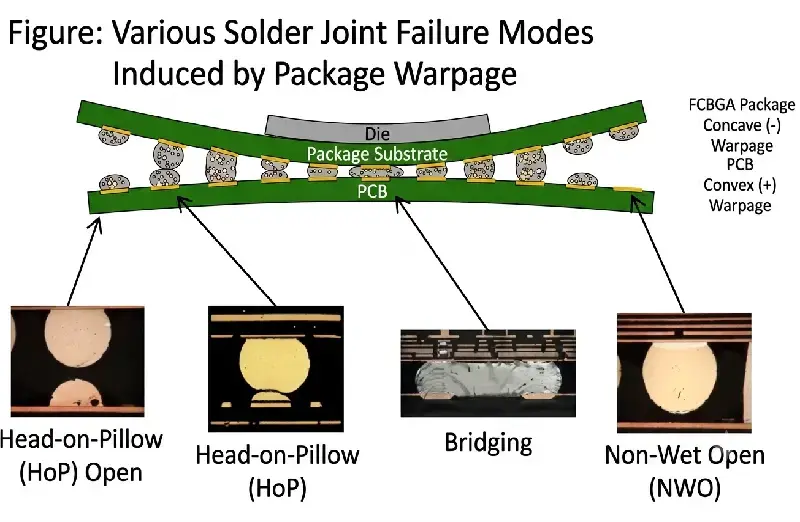
- Diagram of solder joint failure modes caused by package warpage, including head-on-pillow open, head-on-pillow, bridging, and non-wet open defects
- (Images sourced from the web. If you believe any image infringes your copyright, please contact us for removal.)
Core Advantages of Glass Substrate
- Lower CTE: Reduces warpage risk in large packages during manufacturing and operation, improving yield.
- Higher interconnect density: Excellent surface flatness supports finer-pitch routing and higher-density through-glass vias (TGV) — see our companion article for a deep dive.
- Better electrical performance: Glass has lower dielectric loss than common organic materials, benefiting high-frequency signal transmission — one reason glass substrate technology draws interest from both high-performance computing and photonic integration.
| Indicator | Silicon | Organic Materials (ABF/BT) | Packaging-Specific Glass (Borosilicate) |
|---|---|---|---|
| Dk (1-10GHz) | ~11.9 | ~3.5-4.7 | ~4.5-5.5 |
| Df (Loss) | High, and deteriorates with frequency/carrier effects | ~0.005-0.015 | ~0.002-0.003 |
| Signal Propagation Speed | Slow | Fast | Medium |
- Key Term Notes:
- Dk: Dielectric Constant (relative permittivity), a core parameter characterizing the dielectric properties of materials
- Df: Dielectric Loss (loss tangent), reflecting the energy loss of dielectric materials under electromagnetic field action
- ABF: Ajinomoto Build-up Film, a common organic substrate material for semiconductor packaging
- BT: Bismaleimide Triazine, another widely used organic substrate material
- Borosilicate glass: A special glass material with excellent electrical insulation and thermal stability, used for high-performance chip packaging
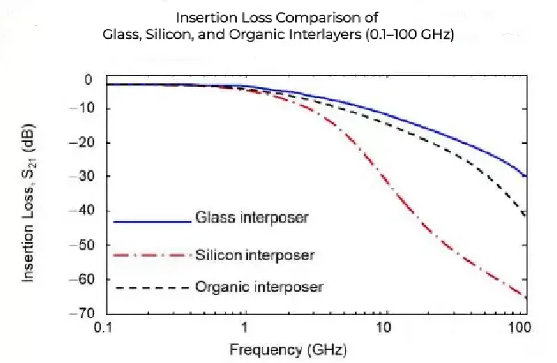
- Insertion loss comparison chart of glass, silicon, and organic interposers from 0.1 to 100 GHz showing glass has the lowest signal loss at high frequency
- (Images sourced from the web. If you believe any image infringes your copyright, please contact us for removal.)
- Panel-level packaging scalability: Glass panels can be processed at larger sizes, potentially lowering per-unit-area manufacturing cost, aligning with the large-area packaging needs of AI chips and HBM stacking.
The Overlooked Cost: Glass Substrates Aren't Free of Trade-offs
Most introductory content emphasizes only the "lower CTE, flatter surface" side of glass substrates. The real engineering difficulty lies in what those advantages cost:
- Brittleness and line-compatibility issues: Glass is a brittle material, with far less bend and impact tolerance than organic substrates or toughened silicon. Most existing handling, placement, and dicing equipment designed for organic substrates cannot be directly reused for glass panels. Edge chipping is a particular risk during dicing and handling, requiring dedicated panel-handling equipment and line layouts.
- "Bulk CTE match" does not mean "zero local stress": Glass substrates have an overall CTE closer to silicon — an advantage relative to the die. But inside a through-glass via (TGV), the fill material is typically copper, and the CTE mismatch between copper and glass is actually significant. This means stress concentrates at the via-glass interface during thermal cycling, potentially creating a new reliability weak point. This is exactly why TGV via design and metallization have become an independent area of technical work — not simply "port over the organic substrate's via process."
- A dual ramp in equipment and yield: Glass substrate commercialization is not just a material swap — it requires rebuilding laser processing equipment, inspection tools, and yield models from scratch. Larger panels mean a higher probability that at least one fatal defect appears somewhere on the panel, a yield-economics challenge common to any move from wafer-level to panel-level advanced packaging — not unique to glass, but amplified by glass's brittleness.
Two Technology Paths: Glass Core Substrate vs. Glass Interposer
Glass substrate technology currently splits into two main paths: replacing the substrate's core layer with glass — known as glass core substrate — and replacing the silicon interposer with glass — known as glass interposer. The two differ meaningfully in application scenario, process difficulty, and commercialization timeline. We break this down in detail in our companion article, "Glass Core Substrate vs. Glass Interposer: Key Differences."
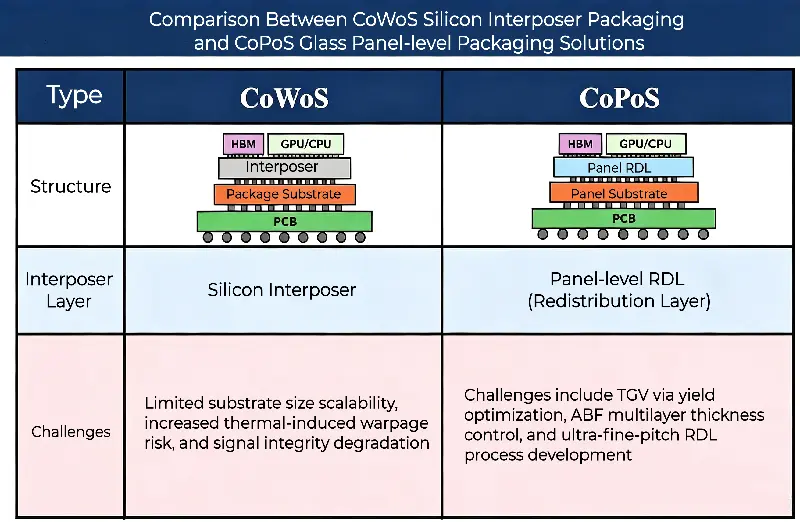
- Comparison diagram of CoWoS silicon interposer packaging structure versus CoPoS glass panel-level packaging structure
- (Images sourced from the web. If you believe any image infringes your copyright, please contact us for removal.)
Primary Applications
- AI accelerators and high-performance computing (HPC) chip packaging
- High-bandwidth memory (HBM) stack packaging
- 5G/6G communication infrastructure chips
- Automotive-grade electronics (where dimensional stability and reliability requirements are stricter)
Why Now: The Packaging Economics Behind a Slowing Moore's Law
Glass substrate is not a brand-new technology — related exploration has been underway for nearly a decade. What has pushed it into the spotlight over the last two to three years is not simply "AI needs more compute." The deeper driver is a structural shift in process economics: as transistor scaling approaches physical limits, the marginal cost of squeezing more performance out of pure process shrinks keeps rising. The industry has increasingly shifted its performance-scaling bets to the packaging layer — chiplets, larger interposers, and higher-density interconnects — moving problems that used to be solved by process shrink into the packaging domain instead. Traditional silicon interposers are constrained by wafer size (e.g., the reticle limits tied to 300mm wafers), placing a ceiling on how many dies and how much area a single package can carry. Glass panels can be processed at areas far larger than a wafer, theoretically lowering the per-unit interconnect cost. In other words, the rise of glass substrate is fundamentally a step the industry has to take in the relay race between "packaging" and "process" to keep the performance curve going — not merely a technology preference of a handful of chipmakers.
Where the Industry Stands Today
Chipmakers including Intel and Samsung, along with materials and equipment suppliers such as Absolics, SKC, AGC, Corning, and JNTC, are advancing pilot and commercialization efforts for glass substrates and glass interposers. See our companion article, "Glass Substrate Supply Chain and Key Players," for a full landscape breakdown.
Frequently Asked Questions
Is glass substrate the same as silicon substrate?
No. Silicon substrate typically refers to a silicon interposer or through-silicon via (TSV) approach. Glass substrate replaces organic or silicon material as the packaging carrier with glass — the two differ in material properties and process path.
Is glass substrate already in mass production?
As of now, glass substrate overall remains in a small-to-mid-volume production validation stage; broad commercial adoption is expected to require a longer maturation cycle.
Will glass substrate replace organic substrate?
In the near term, the two are more likely to coexist: organic substrates retain an advantage in cost-sensitive applications, while glass substrates are landing first in high-end AI/HPC packaging.
What is the biggest engineering challenge for glass substrate?
It's not the electrical or thermal properties of the material itself, but the line-compatibility issues caused by brittleness, along with the localized CTE mismatch between the copper via fill and the glass substrate — a nuance often obscured by "bulk CTE match" marketing language, yet exactly the part reliability engineering needs to solve.
Is the rise of glass substrate purely driven by AI demand?
AI compute demand is the direct trigger, but the deeper cause is diminishing marginal returns from process node scaling. The industry needs the packaging layer — larger area, higher-density interconnects — to keep extending the performance curve, and glass substrate is one of the key material options in that structural shift.
NextPCB provides advanced PCB manufacturing capabilities, including high-density interconnect (HDI), high-frequency/high-speed materials, and support for emerging packaging-adjacent technologies. If your project involves these capabilities, explore NextPCB's advanced PCB manufacturing capabilities.