
 Surface


Julia Wu - Senior Sales Engineer at NextPCB.com

 NextPCB Capabilities
Printed Circuit Boards
NextPCB Capabilities
Printed Circuit Boards
 PCB Assembly
 Layer Buildup
 SMD-Stencils
 PCB Design-Aid & Layout
 Mechanics
 Quality
 Drills & Throughplating
 Factory & Certificate
 PCB Assembly Factory Show
Certificate
PCB Assembly Factory Show
Certificate
Support Team
Feedback:
support@nextpcb.com


Table of Contents
In the second half of 2025, as AI compute shifts from the cloud to the edge, applications like smart camera modules, industrial AI boxes, and vehicle edge computing units demand unprecedented "instantaneous high performance." The increasing integration and speed of chips rapidly surpass the limitations of traditional PCB design and manufacturing methods.
Role Shift: From Procurement to Engineering Leadership
The change in search behavior reflects a profound shift in decision-making leadership. Previously, B2B procurement focused on manufacturing costs such as "unit price, lead time, and whether HDI is possible." Today, driven by the emergence of high-performance challenges, hardware engineers are leading the solution selection. Their core concern is: "Can the supplier help me solve complex SI/thermal design problems?"
This shift demands that NextPCB be more than just a fabrication facility; we must be a provider of customized solutions capable of overcoming high-performance difficulties. Traditional 4-6 layer rigid boards or standard HDI are no longer sufficient; engineers need to enter a more specialized "solution exploration" phase.
>> Recommend reading: HDI PCB Trends in 2026: Innovations, Market Demand, Sustainability, and Challenges
When engineers begin searching for “HDI PCB for Edge AI Accelerator,” they are already grappling with two critical engineering issues:
Pain Point 1: Signal Integrity (SI) under Extreme Density.
Edge AI chips (such as NPUs, FPGAs) utilize high-density BGA packages with signal rates often reaching PCIe Gen4/5. This requires the PCB to achieve the shortest, reflection-free, and precisely impedance-controlled transmission paths within minimal routing space.
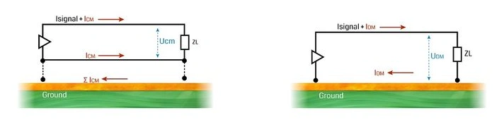
Current return paths and common-mode vs differential-mode currents in a high-speed HDI PCB for edge AI accelerator signal integrity
Pain Point 2: Localized High Heat.
Powerful computing concentrated in small volumes makes thermal management a bottleneck that limits chip performance and long-term reliability.
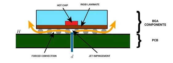
Localized hotspot cooling of a BGA package on an edge AI accelerator HDI PCB, showing forced convection and jet impingement thermal path
Any-layer HDI, a technology where connections between any two adjacent layers can be made via laser blind vias, is the physical foundation for resolving edge AI accelerator issues and ensuring system reliability.
>> Before discussing Any-layer HDI in detail, it is helpful to understand how HDI PCB stackups are commonly classified (such as 1+N+1, 2+N+2, and Any-layer structures). A clear overview can be found in: Common HDI Stackup Types (1+N+1, 2+N+2 and More)
The Any-layer structure allows signal layers to connect between any adjacent layers using micro-vias. This enables complex BGA fanout paths to traverse vertically, maximizing horizontal routing layer utilization and effectively solving the problem of insufficient signal layers—the only solution for achieving ultra-high-density routing.
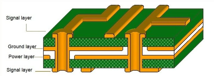
Multilayer HDI PCB cross-section with balanced signal, ground and power layers for Any-layer edge AI accelerator routing
Compared to traditional mechanical through-hole vias, micro-vias significantly shorten the signal path, fundamentally reducing reflection, crosstalk, and parasitic capacitance at the via point, eliminating the Via Stub effect, and ensuring high-speed signal integrity (SI assurance).
> Recommend reading: Fast Positioning of Signal Integrity Problems in High Speed Circuit Design
The Any-layer structure allows us to densely deploy arrays of thermal vias directly beneath the hot spots of the chip and combine them with large inner-layer copper planes. This creates the shortest, most direct board-level thermal path—the starting point for solving localized edge heat (Thermal Path).
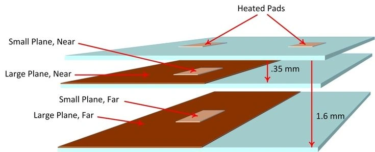
Board-level thermal spreading from heated pads into small and large copper planes inside a multilayer HDI PCB for edge AI accelerators
Entering the "Parameter Validation" phase, B2B procurement and R&D engineers focus on the most rigorous process indicators. NextPCB’s exceptional precision manufacturing capabilities ensure stable mass production experience for the following extreme parameters:
| Key Technical Parameter | AI Accelerator Requirement (Hyper-niche Spec) | Engineering Significance |
|---|---|---|
| Layer Count | 10-12 Layers | Ensures sufficient Power/Ground planes, stable power supply, and effective EMI suppression. |
| HDI Structure | Any-layer (Arbitrary Interconnect) | Ensures the shortest fanout path beneath the BGA, meeting PCIe Gen5/6 high-speed signal requirements. |
| Line/Space (L/S) | 3/3mil (75um/75um) | Achieves high-density routing, guaranteeing the precision of impedance control and routing space for critical signals. |
| Via Technology | Blind/Buried Vias | Eliminates the Via Stub effect, reducing signal reflection and crosstalk. |
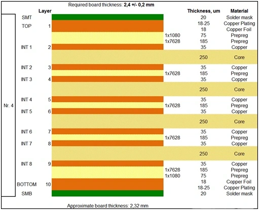
Example 10-layer Any-layer HDI PCB stack-up for edge AI accelerator design, showing signal, ground and power layer distribution
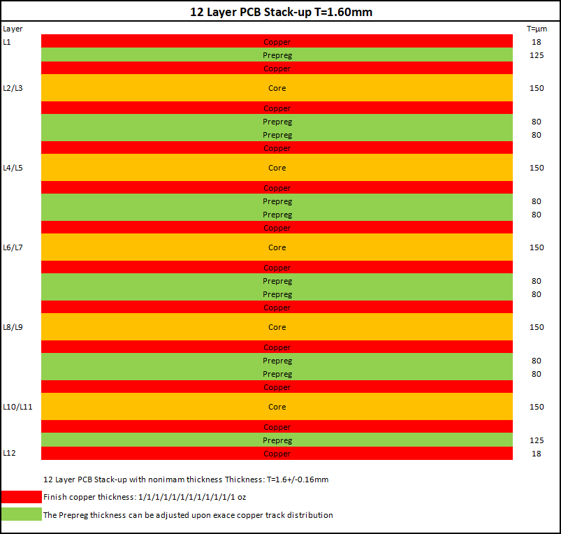
12-layer HDI PCB stack-up T=1.60 mm with detailed copper and prepreg thickness for edge AI accelerator boards
NextPCB advocates for Thermal Co-design and SI Co-design with customers, treating the PCB as a system-level solution. Here are three core dimensions to focus on when selecting a supplier:
This is the supplier's "hard threshold." You must confirm their stable mass delivery capability for L/S 3/3mil, up to 3-stage blind/buried vias, and 12+ layer Any-layer stacking to ensure the design is not compromised by manufacturing constraints.
Especially for typical high-speed interfaces like PCIe Gen4/5, LPDDR4/5, and SerDes, the supplier must offer professional collaboration services:
Impedance Dimension: Capability to flexibly select Low-Loss/Ultra-Low Loss dielectric materials with low Dk/Df.
Via Design: Utilizing processes like Via-in-Pad (VIP) + Resin Filling + Copper Cap to ensure signal quality from the source.
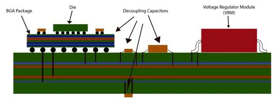
Power integrity layout of BGA package, decoupling capacitors and VRM on an edge AI accelerator HDI PCB forming a low-impedance PDN
Engineering Collaboration Tip: For PCIe Gen4/5 differential pairs, it is advisable to communicate the target impedance, routing layer count, and via structure with the supplier early on, leveraging simulation data to perform stack-up reverse engineering.
For thermal design, confirm the supplier's manufacturing capability supports the construction of the following thermal paths:
Board-Level Thermal Path: Ensures heat is transferred from the chip pad → Via-in-Pad (thermal filling) → large inner copper planes → ultimately guided to the radiator/casing contact surface.
Material Selection: Ability to select High-Tg (Glass Transition Temperature) materials for high-power density areas to balance reliability and performance.
System-Level Thermal Integration: Ensure the PCB's thermal copper (such as ground or power planes) can effectively connect to the casing's thermal contact points to transfer heat to the enclosure for passive dissipation.
NextPCB deeply understands the urgency of the next-generation AI hardware iteration. We have profoundly integrated manufacturing capabilities with engineering collaboration to help you capture the edge AI hardware market opportunities in the second half of 2025.
NextPCB has stable mass production experience with the high-quality Any-layer HDI and can flexibly configure various low-loss materials according to your SI needs. We ensure the consistency and reliability of high-layer-count HDI through a comprehensive quality management system and full-process online inspection.
We offer deep engineering collaboration, intervening early in the design process:
Design Optimization (DFM/DFA): We participate early in stack-up and DFM (Design for Manufacturability) review, and can provide DFA (Design for Assembly) file support, saving customers at least 3 days of waiting time.
High-Speed/Thermal Integrated Advice: Provide integrated "High-Speed + Thermal" layer advice, including preliminary layout and layer Review for PCIe, DDR, and Power Distribution.
We understand that the biggest fear in high-precision design is "it works for the prototype, but is unstable in mass production." NextPCB commits that production from Prototype to Small Batch and Mass Production always occurs on the same process window and the same equipment chain. This consistency is crucial for ensuring the stable performance and reliability of your Edge AI accelerator PCB design. We warmly welcome you to visit our manufacturing facilities to witness this process firsthand.
Immediate Call to Action: Boost Your AI Accelerator Project Performance
Q: What is Any-layer HDI PCB and why is it critical for edge AI accelerators?
A: Any-layer HDI allows vertical micro-via connections between any two adjacent layers. This freedom is essential for routing highly complex BGA packages (like NPUs), enabling the shortest possible high-speed signal paths, which is critical for maintaining signal integrity (SI) and maximizing routing density.
Q: How does Any-layer HDI help with thermal management of edge AI chips?
A: The Any-layer structure enables the creation of dense arrays of thermal vias directly beneath the chip pads (Via-in-Pad). These micro-vias efficiently transfer heat from the chip's base layer to the inner copper planes, establishing a direct, low-resistance thermal conduction path at the board level.
Q: What stack-up and line/space do I need for PCIe Gen4/Gen5 on AI accelerator boards?
A: For Gen4/Gen5 speeds, you typically require high layer counts (10-12 layers) with multi-stage blind/buried vias and tight Line/Space (L/S) of 3/3mil. Crucially, low-loss or ultra-low loss dielectric materials must be used, and the stack-up design must be co-engineered with the manufacturer to ensure impedance control and consistent signal performance.
Q: How to choose a PCB manufacturer for Any-layer HDI with 3/3mil capability?
A: Look beyond mere capability. A reliable supplier must offer robust engineering co-design services (DFM/stack-up review), demonstrate high-volume consistency from prototype to mass production on the same equipment, and possess established quality certifications to ensure the reliability of the complex 3/3mil Any-layer process.

Still, need help? Contact Us: support@nextpcb.com
Need a PCB or PCBA quote? Quote now

