



Julia Wu - Senior Sales Engineer at NextPCB.com

 NextPCB Capabilities
Printed Circuit Boards
NextPCB Capabilities
Printed Circuit Boards
 PCB Assembly
 Layer Buildup
 SMD-Stencils
 PCB Design-Aid & Layout
 Mechanics
 Quality
 Drills & Throughplating
 Factory & Certificate
 PCB Assembly Factory Show
Certificate
PCB Assembly Factory Show
Certificate

Support Team
Feedback:
support@nextpcb.com


Eight layers is the point where most designers outgrow a 6-layer board: enough copper for a full ground cage, a dedicated power plane pair, and the routing density that dense BGAs and mixed-signal designs demand. This guide walks through the standard 8-layer lamination structures NextPCB supports, how dielectric thickness affects symmetry and impedance, and how to pull manufacturing-verified stackup data before you finalize your layout.
| Standard Configurations | 6 lamination schemes (see below), signal-layer count from 4 to 6 depending on plane coverage |
|---|---|
| Final Board Thickness Options | 1.0mm, 1.2mm, 1.6mm, 2.0mm, 2.5mm |
| Outer Copper Weight | 0.5oz (0.018mm) or 1oz (0.035mm) |
| Typical Dielectric per Layer | As low as ~0.135mm (core) in thinner/high-symmetry builds |
| Default Calc. Parameters | 0.5 mil / 0.0127mm solder mask over trace, 1.2 mil / 0.0305mm over substrate, Er = 3.5 |
| Impedance Tolerance | ±5% on advanced PCB builds, TDR-verified |
| HDI Upgrade Path | 1+N+1, 2+N+2 and any-layer interconnects with laser-drilled blind/buried vias if routing density later exceeds standard through-hole |
See the full lamination structures below, or query your exact stackup by thickness and copper weight.
A 6-layer board typically gives you four signal layers around one ground-power pair, which is enough for moderate-density digital designs. Once a design adds a second high-speed bus, a denser BGA (0.5mm pitch and below), or mixed digital/RF/power sections that need isolation from each other, four signal layers stop being enough without pushing trace widths and spacing below what the fab can reliably hold. Moving to 8 layers adds the copper needed for a dedicated ground cage, a real power-ground plane pair for decoupling, and enough signal layers to route without breaking reference planes mid-trace.
The trade-off is lamination cycles: an 8-layer board needs two full press cycles instead of one, which adds cost and lead time versus a 6-layer build. The stackup you choose determines how much of that extra copper actually goes toward signal integrity versus just adding routing room.
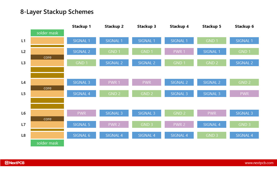
NextPCB's standard process supports several proven 8-layer lamination structures. Each one trades signal-layer count against reference-plane coverage differently, so the right choice depends on whether your priority is routing density, power integrity, or EMI suppression.
| Layer | Stackup 1 | Stackup 2 | Stackup 3 | Stackup 4 | Stackup 5 | Stackup 6 |
|---|---|---|---|---|---|---|
| L1 | Signal 1 | Signal 1 | Signal 1 | Signal 1 | GND 1 | Signal 1 |
| L2 | Signal 2 | GND 1 | GND 1 | PWR 1 | Signal 1 | GND 1 |
| L3 | GND 1 | Signal 2 | Signal 2 | GND 1 | GND 2 | Signal 2 |
| L4 | Signal 3 | PWR 1 | PWR | Signal 2 | Signal 2 | GND 2 |
| L5 | Signal 4 | GND 2 | GND 2 | Signal 3 | Signal 3 | PWR |
| L6 | PWR | Signal 3 | Signal 3 | GND 2 | PWR | Signal 3 |
| L7 | Signal 5 | PWR 2 | GND 3 | PWR 2 | Signal 4 | GND 3 |
| L8 | Signal 6 | Signal 4 | Signal 4 | Signal 4 | GND 3 | Signal 4 |
Six signal layers against a single ground plane and a single power plane. This is essentially the disadvantages of two different 6-layer approaches combined in exchange for routing room. It only makes sense when impedance and signal integrity requirements are genuinely low; otherwise the limited reference-plane coverage will cause return-path problems.
Adds a full power-ground plane pair (L4/L5) and gives every signal layer an adjacent reference plane. This is the practical default for designs that need real power integrity without going as far as a dedicated EMI shield structure.
Trades one of the two power planes in Stackup 2 for an extra ground layer, creating ground references above and below the inner signal layers. Shorter return paths and stronger EMI suppression, at the cost of a second dedicated power plane.
A direct extension of a 6-layer plane-pair design: two full plane pairs create an isolated stripline environment for the inner signal layers while keeping the buildup symmetric around the center, and two full layers are available for power distribution.
Both reference ground on the outer layers rather than routing signal there, which is useful when the top and bottom layers are needed mainly for shielding, component pads, or coating flatness rather than high-speed routing. The single power layer stays centralized (L6) in both configurations.
You can pull the exact core, prepreg, and copper-weight makeup for each of these — matched to your target board thickness — from NextPCB's Impedance Control Stackups tool, and read the general reasoning behind stackup selection across layer counts in Choosing High-Speed PCB Stackups from 4 to 10 Layers.
Some 8-layer and higher-layer-count builds use multiple stacked prepregs paired with thinner cores, which makes the core dielectrics thinner than the prepreg areas. That construction lets you place symmetrical plane pairs both on either side of the board's center and directly at the center, keeping maximum mechanical symmetry through the whole stack. In thinner boards and higher layer counts, individual dielectric layers can easily fall below 0.2mm — which is exactly what you want for tight coupling and predictable return-path management on high-speed layers.
| Layer | 8-layer, 1.6mm board | 8-layer, 1.0mm board |
|---|---|---|
| L1 (outer) | 0.077mm, 1080 | 0.077mm, 1080 |
| L2 (core) | 0.135mm | 0.135mm |
| L3 | 0.23mm + 0.23mm, 7628H | 0.16mm, 1506 |
| L4 (core) | 0.135mm | 0.135mm |
| L5 | 0.23mm + 0.23mm, 7628H | 0.16mm, 1506 |
| L6 (core) | 0.135mm | 0.135mm |
| L7 (outer) | 0.077mm, 1080 | 0.077mm, 1080 |
Note how the 1.0mm build swaps the thicker 7628H double-prepreg for a single 1506 layer — same core structure, thinner glass style, to hit the tighter overall thickness while keeping the stack symmetric.
The decision usually comes down to three factors:
As a rule of thumb: if your current 6-layer layout is failing DRC on trace/space or you're fighting for a second reference plane, 8 layers is usually the more predictable path forward rather than pushing a 6-layer stackup past what the fab can hold reliably.
Theoretical stackup diagrams are a starting point, but the numbers that actually matter — cured core and prepreg thickness, resin content, dielectric constant — come from the fabricator's real material set. NextPCB's Impedance Control Stackups tool lets you pull that data directly before you finalize your design:
The tool's calculation model already accounts for solder mask (0.5 mil / 0.0127mm over trace, 1.2 mil / 0.0305mm over substrate, Er = 3.5), and returns final reference values after coating rather than bare-copper impedance — so the numbers you get map more closely to what a TDR measurement will show post-fabrication.
For the broader reasoning behind stackup selection across layer counts — not just 8 layers — see Choosing High-Speed PCB Stackups from 4 to 10 Layers.
When you're comparing fabricators for an 8-layer, impedance-controlled build, the questions that actually predict a smooth build are:
For 100% production precision beyond the tool's pre-layout estimate, a free HQDFM check against your actual Gerber files is the standard next step before ordering.
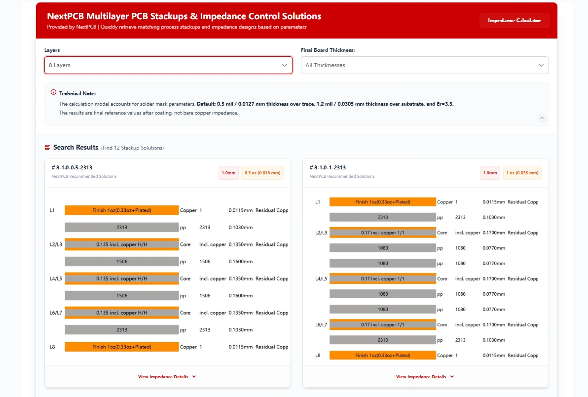
NextPCB Multi-layer PCB Stack-up Design & Impedance Control Solutions
NextPCB's standard 8-layer process supports 1.0mm, 1.2mm, 1.6mm, 2.0mm, and 2.5mm finished thicknesses, each with multiple core/prepreg combinations and copper weight options.
Tools like NextPCB's Impedance Control Stackups system use standard analytical formulas for typical PCB geometries, which are highly accurate for pre-layout evaluation. Actual results can vary slightly with etching factors and resin content during mass production — production impedance is managed to ±5% with TDR-verified reports, and a free HQDFM check gives 100% production-verified numbers before you order.
Yes, but the increase isn't fixed — it scales with the extra lamination cycle and drilling pass, plus your specific thickness, copper weight, and quantity. Comparing instant quotes for both layer counts on your actual board dimensions gives a more accurate answer than a general rule of thumb.
Yes. The standard stackup tool covers FR-4-based builds; for Rogers, Megtron, or other hybrid material stackups, contact the manufacturer's engineering team directly to confirm materials and lead time.
Standard 8-layer stackups are through-hole by default, but most manufacturers — including NextPCB — support complex HDI structures such as 1+N+1 and 2+N+2 with laser-drilled blind and buried vias if your design needs them.
Confirm they publish real, queryable stackup data (not just a generic diagram), support your target thickness and copper weight out of the box, and can walk you into HDI or custom material stackups if a later revision needs it — without switching fabricators. A free HQDFM check before ordering is a good sign the manufacturer verifies designs against actual process capability rather than just accepting Gerbers as-is.

Still, need help? Contact Us: support@nextpcb.com
Need a PCB or PCBA quote? Quote now

