Miniaturization Meets Mass Market
The Consumer Electronics (CE) market is defined by relentless innovation, shrinking footprints, and lightning-fast product cycles. From next-generation smartphones and wearables to smart home devices and IoT gateways, success hinges on two critical factors: fitting maximum functionality into minimum space, and hitting the market window before the competition.
NextPCB understands the unique demands of this highly competitive sector. Our expertise is rooted in enabling the technologies that drive modern CE, focusing on advanced manufacturing techniques that ensure both performance and cost-effectiveness at scale. >>> Get an Instant PCB Quote
The PCB Challenges of Consumer Electronics
Designing the electronics for modern consumer devices presents several unique manufacturing hurdles that go beyond standard PCB fabrication:
- Extreme Miniaturization: Devices like earbuds and smartwatches require micro-fine pitch components and incredibly dense circuit routing.
- High-Speed Data: Wireless and networking features demand excellent signal integrity and often require high-frequency materials (e.g., Rogers) to maintain performance.
- Cost & Scalability: The Bill of Materials (BOM) must be optimized for volume production without sacrificing reliability.
Advanced Solutions for CE Devices
Our manufacturing capabilities are specifically engineered to address the miniaturization and complexity required by consumer electronics:
| Technical Solution |
Application in Consumer Electronics |
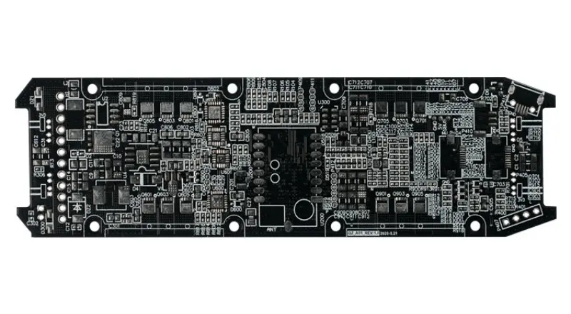
HDI PCBs
(High Density Interconnect) |
The foundation for smartphones, tablets, and advanced cameras. HDI utilizes microvias to maximize routing density, drastically reducing board size. |
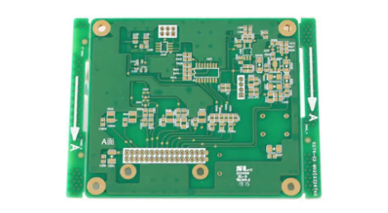
| Rigid-Flex and Flexible PCBs |
Essential for wearables and compact cameras, allowing circuits to bend and fit into highly irregular, space-constrained enclosures. |
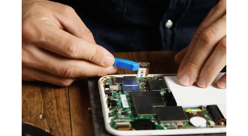
| Advanced PCB Assembly |
Handling ultra-fine pitch components (e.g., BGA, 01005s) common in portable electronics, ensuring high yield rates for volume production. |
Speed and Scale: Your Competitive Edge
In Consumer Electronics, the first to market often captures the largest share. NextPCB is built for speed and rapid iteration:
- Fast Prototyping: We provide rapid PCB prototyping services, allowing engineers to test and validate designs quickly before committing to mass production.
- Optimized Turnkey Service: Our integrated manufacturing process includes PCB assembly and efficient BOM sourcing, minimizing logistical delays and controlling overall cost.
- Reliability for Mass Production: All our processes adhere to UL and RoHS standards, ensuring your product is compliant and reliable for global distribution.
>>> See NextPCB Quality Certifications and Test Reports
PCB Capabilities Supporting This Industry
Turnkey PCB Assembly
Complete sourcing and assembly services optimized for cost-sensitive consumer products.
View Assembly Services
Frequently Asked Questions
What PCB technologies are best for wearable devices?
Rigid-flex and HDI (High Density Interconnect) PCBs are essential for wearables. They allow circuits to fold into compact shapes like wristbands or glasses while maintaining the high performance needed for sensors and connectivity.
Can NextPCB handle high-volume consumer electronics orders?
Yes. NextPCB specializes in scaling from prototype to mass production. We offer optimized pricing structures and logistics specifically designed for high-volume consumer electronics manufacturing.
Do you provide assembly for fine-pitch components?
Absolutely. Our advanced assembly lines are equipped to handle ultra-fine pitch components, including 01005 passives and BGAs, which are standard in modern smartphones and compact IoT devices.
Partner with NextPCB for Consumer Electronics
Ready to turn your innovative concept into a market-ready product? Partner with NextPCB for the speed, quality, and scale required by the Consumer Electronics industry. >>> Upload Your Design & Get a Quote
Related PCB Application Industries

 NextPCB Capabilities
 PCB Assembly
 Layer Buildup
 SMD-Stencils
 PCB Design-Aid & Layout
 Mechanics
 Quality
 Drills & Throughplating
 Factory & Certificate
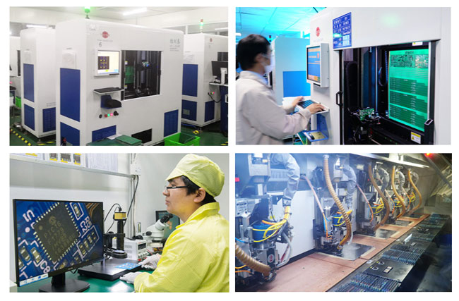
 PCB Assembly Factory Show
Certificate
PCB Assembly Factory Show
Certificate
 NextPCB Capabilities
 PCB Assembly
 Layer Buildup
 SMD-Stencils
 PCB Design-Aid & Layout
 Mechanics
 Surface
 Quality
 Drills & Throughplating
 Factory & Certificate