
 Surface


Zhang

 NextPCB Capabilities
Printed Circuit Boards
NextPCB Capabilities
Printed Circuit Boards
 PCB Assembly
 Layer Buildup
 SMD-Stencils
 PCB Design-Aid & Layout
 Mechanics
 Quality
 Drills & Throughplating
 Factory & Certificate
 PCB Assembly Factory Show
Certificate
PCB Assembly Factory Show
Certificate
Support Team
Feedback:
support@nextpcb.com


Introduction
The schematic diagram is the logical representation of an electronic system's function, distinct from wiring or layout diagrams. It defines the electrical connectivity between components and serves as the core source for PCB layout and manufacturing deliverables.
Key takeaways: 1) A schematic only expresses functional logic, clearly distinguishing it from the physically focused Wiring Diagram and PCB Layout. 2) Adherence to IEC/IEEE international standards and consistent Reference Designators (RefDes) is fundamental for unambiguous collaboration and manufacturing. 3) A rigorous drafting process must include Electrical Rules Check (ERC) and Netlist generation to ensure data precision, directly impacting Design for Manufacturing (DFM) and In-Circuit Testing (ICT).
Reader Benefits: Readers will learn how to embed DFM constraints using schematic tools (ERC/Net Class), master an actionable design and verification workflow, and access a comprehensive design checklist.
Contents
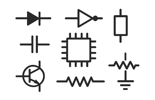
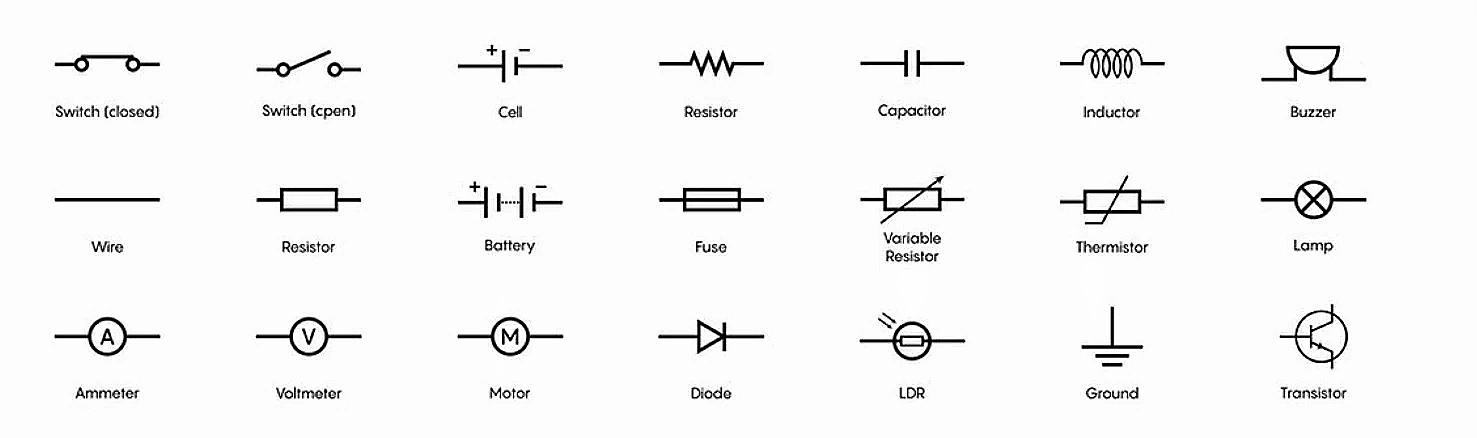
The Schematic Diagram, or circuit diagram, is the logical blueprint of an electronic system as a functional entity. It is a highly abstract and symbolic representation that uses standardized graphic symbols for physical components (such as resistors, ICs, and transistors) and lines to represent the electrical connection paths between them.
The core principle of a schematic is to convey functional connectivity—which pin connects to which pin—without regard for the actual physical arrangement of these components in the final device. This abstraction allows engineers to easily understand and analyze the circuit's function without being distracted by physical layout constraints.
A schematic is fundamentally composed of three elements:
While a schematic is known for its abstraction and omission of irrelevant details, when created for manufacturing or simulation, a balance must be maintained between functional clarity and necessary physical details. For modern ECAD (Electronic Computer-Aided Design) tools, the component symbol must include all physical pins on the device; even unconnected or reserved pins (NC pins) need to be clearly marked. Omitting these physical details in the schematic symbol can cause errors or failures during subsequent netlist generation and footprint mapping. Therefore, a schematic created for manufacturing must faithfully reflect the component's full physical interface information while maintaining logical clarity.
A common mistake for novice designers is confusing the logical schematic with documentation that reflects physical location. Defining the boundaries of the schematic is critical:

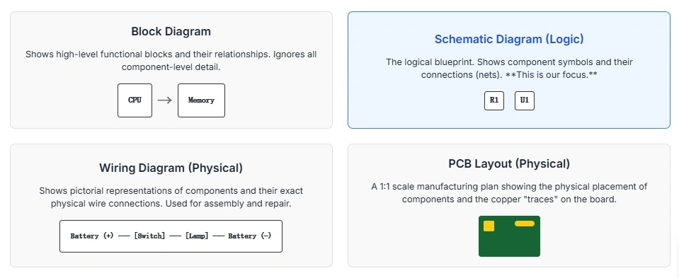
Understanding the distinctions between various electronic diagrams is fundamental for effective hardware team communication, ensuring the correct documentation is used for different tasks such as debugging, assembly, or manufacturing.
> Recommend reading: PCB Schematic vs PCB Layout
The table below details the distinct roles played by each major drawing type throughout the product lifecycle.
| Diagram Type | Purpose | Reflects Physical Location | Primary Output/File | Primary Audience | Typical Use Case |
|---|---|---|---|---|---|
| Schematic Diagram | Defines logical electrical connectivity and function. | No (optimized for functional clarity and signal flow). | Netlist, Bill of Materials (BOM) | Electrical Engineer, Circuit Debugging, Layout Input | Design creation, simulation, code review |
| Block Diagram | Shows the organizational relationship between functional units. | High-level organizational structure only. | System Architecture Document | System Architect, Project Manager | Project planning, high-level functional overview |
| Wiring Diagram | Illustrates physical point-to-point connections needed for assembly or maintenance. | Yes (focuses on physical routing of cables/harnesses). | Assembly instructions | Wiring/Assembly Technician | Harness assembly, field service/repair |
| PCB Layout | Defines the precise physical placement of components and copper routing on the board. | Yes (exact component location and trace paths). | Gerber Files, ODB++ | PCB Manufacturer, Layout Engineer | Manufacturing and Assembly (SMT/THA) |
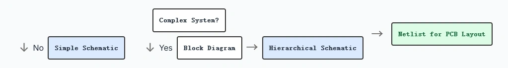
System complexity is the determining factor for the starting point and structure of the design:
Adherence to established drafting standards is mandatory in professional engineering documentation. Standards eliminate ambiguity, simplify collaboration across international teams, minimize manufacturing errors, and facilitate maintenance and reverse engineering.
A Reference Designator (RefDes) is a unique identifier assigned to each component (e.g., R101, C22). Its letter prefix indicates the component type.
When selecting RefDes letters, although standards exist (like IEEE 315), different companies or projects may have internal agreements. Internal company conventions take priority, maintaining consistency is paramount. For instance, frequency components should distinguish between passive crystals (Y) and active oscillator modules (X). The key is to ensure that within the entire design (including schematic and PCB Layout), each letter represents a unique component type to avoid ambiguity.
| RefDes | Component Type | Notes/Context |
|---|---|---|
| R | Resistor | Includes Variable Resistors (VR). |
| C | Capacitor | Includes polarized and non-polarized types. Polarized capacitors should use a curved plate symbol for distinction. |
| L | Inductor | Coils, chokes, ferrite beads (sometimes FB). |
| D | Diode | Includes LEDs. In the standard symbol, the bar side is the Cathode (K), and polarity must be clearly marked. LED symbols have "light arrows" pointing outward, and photodiode arrows pointing inward. |
| Q | Transistor | BJT, MOSFET, IGBT. |
| U | Integrated Circuit (IC) | Microcontrollers, op-amps, logic chips. |
| J / P | Connector/Jack/Plug | J is typically used for board-mounted connectors, P for plugs or mating components. |
| FB | Ferrite Bead | Specifically used to suppress high-frequency noise. |
| TP | Test Point | Critical for ICT and functional debugging. |
| Y | Crystal / Resonator | Passive frequency components. |
| X | Oscillator Module | Active frequency components. Some organizations also use U (IC) for clock chips. |
The Title Block transforms a simple drawing into a controlled engineering document, ensuring all stakeholders use the correct version with the right context.
Placement and Consistency: The Title Block is usually placed in the lower right-hand corner of the drawing for easy visibility. Maintaining consistent formatting across all drawings ensures easy recognition and interpretation, especially in multi-engineer collaborative projects.
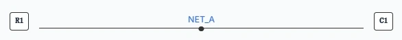
Clear and consistent Net Name conventions are the most important aspect of schematic readability and Netlist accuracy.
Net naming is no longer just annotation; for high-speed design, it is a constraint instruction.
For example, using the _P/_N naming convention for differential pairs enables the software to automatically group them as differential pair objects. This automatic grouping then allows the layout tools to apply complex physical rules like length matching and impedance control. This means the schematic designer defines the logical intent, which is translated into physical constraints via naming conventions. If there are typos or spaces in the net labels, the software will fail to recognize them as the same net, thereby breaking connectivity and preventing the transfer of critical layout rules.
| Standard | Area of Focus | Key Control Domain |
|---|---|---|
| IEC 60617 | International (Global) | Graphical symbols and component representation for electro-technical diagrams |
| IEEE/ANSI 315 | North American Practice | Graphic symbols and standard RefDes system |
| IEC 61082-1 | Documentation Practice | Preparation and structuring of electrical documentation, including Title Block format, revision control, and connection representation. |
Efficiently reading a schematic requires following a standardized, structured methodology, utilizing universally accepted signal flow conventions.
Before analyzing circuit connections, the document's context must first be established:
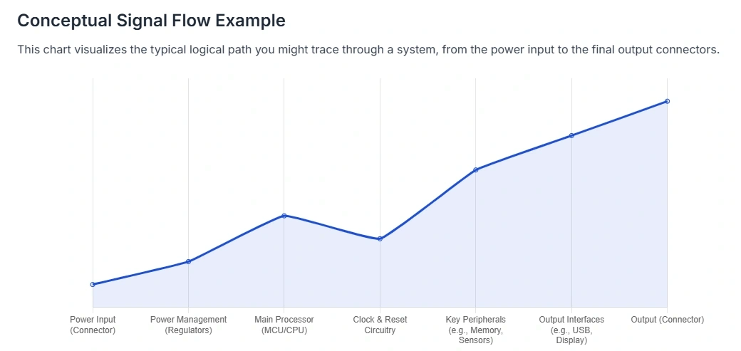
A schematic should be laid out like a book, allowing signal flow to be tracked intuitively.
Effective reading relies on using schematic labels to trace distributed signals, rather than solely depending on connection lines.
Schematic design is a structured engineering process, not merely a drafting exercise. It culminates in generating the Netlist, the authoritative source of connectivity data.
This general seven-step process is applicable to most professional ECAD environments, ensuring the shortest path from concept to deliverable:
The KiCad user workflow is often streamlined:
The process of generating a Netlist in professional ECAD tools involves a compilation step that checks the "unified data model" for logical, electrical, and drafting errors. A robust Netlist is more than just a list of connections; it is the designer's assertion that the schematic fully adheres to the rules defined in the project settings.
A professional schematic is defined not only by its functionality but also by its readability, maintainability, and ability to preemptively flag layout and manufacturing issues.
| Name | Symbol | Factor |
|---|---|---|
| Tera | T | 10^12 |
| Giga | G | 10^9 |
| Mega | M | 10^6 |
| Kilo | k | 10^3 |
| milli | m | 10^-3 |
| micro | µ | 10^-6 |
| nano | n | 10^-9 |
| pico | p | 10^-12 |
Errors in schematic capture often lead to connectivity problems that bypass initial checks but cause catastrophic failures during prototyping or manufacturing.
| Error Type | Description and Impact | Mitigation Strategy |
|---|---|---|
| Missing Junction Dot | Failure to place a clear dot at the intersection of three or more connection lines. Leads to misinterpretation: crossing lines may be incorrectly assumed to be connected or disconnected, corrupting the Netlist. | Always use a junction dot for connections. To maintain clarity, avoid connecting four wires at a single point. |
| Inconsistent Net Naming | Using different name variations for the same signal (e.g., VDD, 3V3, VDD_3V3). The ECAD tool treats them as three separate, unconnected nets (phantom connectivity failure). | Enforce strict naming conventions (e.g., all caps, consistent delimiters). Run ERC to detect single-ended nets that should be connected. |
| Incorrect Polarity | Placing polarized components (such as diodes, LEDs, tantalum, or electrolytic capacitors) in reverse orientation. The diode symbol's bar side is the Cathode (K) and must connect to the lower potential. The positive lead of the capacitor must face the higher voltage. Check the schematic symbol markings (cathode bar, curved plate) for indication. | |
| Missing Power Source | VCC/GND pins on an IC are drawn but not explicitly connected to a designated power port/Net Name. This type of oversight is one of the most common high-risk error types. | Use dedicated, visible power port symbols (e.g., VCC_3V3, GND) for power nets, and thoroughly enable power net integrity checks in the ERC. |
| Missing Constraint Notes | Failure to add annotations or directives for high-speed nets requiring specific Layout rules (e.g., "Differential Pair: 100-ohm impedance, requires length matching"). | Use schematic directives or detailed text annotations on relevant nets/buses to guide the layout engineer. |
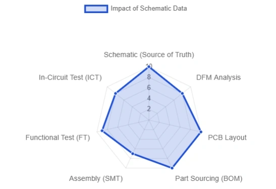
The final output of the schematic is the Design Package, which is the core medium of communication with the PCB manufacturer, assembly house, and test engineering team.
The complete manufacturing package is directly derived from the verified schematic and ECAD project structure.
Manufacturers use Gerber files (physical copper layer data) for fabrication, but they use the Netlist (logical connectivity data) to verify the Gerbers' correctness. If a trace opens or shorts unexpectedly in the Layout but is not visibly obvious in the Gerber files, the IPC-D-356 Netlist check will flag the discrepancy during DFM verification. Thus, the Netlist generated from the schematic acts as the authoritative, "legal" definition of required connectivity. It is the core input for DFM compliance checks and bare board test fixture programming.
> Recommend reading: Scheme-It: An Online Schematic and Diagramming Tool
Try Open Source Online Gerber Viewer from NextPCB
The schematic designer must embed testing and manufacturing requirements into the logical design.
| Question | Answer |
|---|---|
| What is the core difference between a Schematic Diagram and a Wiring Diagram? | A schematic displays electrical connections logically, focusing on function and clarity, not physical location. A Wiring Diagram shows the physical routing of wires and components for assembly purposes. |
| What standards must a schematic follow? | Schematics should primarily follow IEC 60617 (international symbols) or IEEE/ANSI 315 (North American symbols and RefDes), ensuring the symbols and documentation are universally understood. |
| How should the title block be set up? | The Title Block must contain comprehensive project metadata: drawing title, unique drawing number (PN), version/revision, date, and author/approval signatures, typically adhering to standards like IEC 61082-1. |
| What files should be delivered after the schematic is complete? | Core manufacturing deliverables include the final schematic PDF, the Bill of Materials (BOM), and the authoritative Netlist (preferably IPC-D-356 or contained within ODB++). |
| What tools/plugins can automatically check for errors? | The most critical automated check is the Electrical Rules Check (ERC), available in all professional ECAD tools (like Altium, KiCad). ERC identifies connectivity and power net anomalies before the Netlist is generated. |
| Term | Definition |
|---|---|
| Schematic Diagram | A logical representation of a circuit using abstract symbols to define electrical connections (nets). |
| Wiring Diagram | A drawing that shows the physical point-to-point connections used for assembly or harness creation. |
| PCB Layout | The physical design file defining the placement of components, layer stackup, and copper routing on a Printed Circuit Board. |
| Net | An electrical node or connection path between two or more component pins, identified by a unique net label. |
| RefDes (Reference Designator) | The unique alphanumeric identifier assigned to each component in the schematic (e.g., R5, U1). |
| ERC (Electrical Rules Check) | An automated validation tool run on the schematic to ensure logical and electrical integrity. |
| Netlist | A text file derived from the schematic that lists all electrical connections (nets, pins, and RefDes), serving as the core input for PCB Layout and manufacturing testing. |
| Title Block | The standardized data block on an engineering drawing that contains necessary document control information (revision, date, title, part number). |
| BOM (Bill of Materials) | The authoritative list of all components required for assembly, derived from the schematic component definitions. |
| Diff Pair (Differential Pair) | Two tightly coupled nets (labeled _P and _N) carrying complementary signals, constrained in the schematic to meet specific impedance and length requirements in the Layout. |

Still, need help? Contact Us: support@nextpcb.com
Need a PCB or PCBA quote? Quote now

