
 Surface


The Race to the Bottom (in Microns)

 NextPCB Capabilities
Printed Circuit Boards
NextPCB Capabilities
Printed Circuit Boards
 PCB Assembly
 Layer Buildup
 SMD-Stencils
 PCB Design-Aid & Layout
 Mechanics
 Quality
 Drills & Throughplating
 Factory & Certificate
 PCB Assembly Factory Show
Certificate
PCB Assembly Factory Show
Certificate
Support Team
Feedback:
support@nextpcb.com


The Race to the Bottom (in Microns)
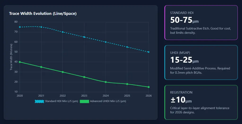
In 2026, Ultra-High Density Interconnect (UHDI) is no longer a "luxury" reserved for flagship smartphones or aerospace. With the proliferation of 6G modules and miniaturized AI edge computing chips, PCB trace widths and spacings (L/S) of 25μm—and even 15μm in some top-tier flagship products—are no longer just lab benchmarks. Understanding the fundamentals of Gerber files for PCBs is the first step in mastering these advanced designs.
However, at the NextPCB DFM Department, we've noticed a critical oversight: while engineers use state-of-the-art EDA tools, the exported Gerber files often rely on "default standards" from twenty years ago. It is essential to review current PCB capabilities to ensure your design data aligns with modern fabrication limits.
For conventional PCBs, this is negligible. For UHDI, insufficient file precision can cause opens, shorts, or impedance mismatches, acting as a "silent killer" of your yield.
Today, we explore the precision requirements for Gerber files in the UHDI era and how to balance "theoretical precision" with "manufacturing reality."
For decades, the default Gerber output was 2:4 (Imperial) or 3:3 (Metric). When comparing older standards like RS274D vs RS274X Gerber, we see how far the industry has moved toward automated data handling, yet resolution settings often lag behind.
In 2026 UHDI designs, we frequently handle 15μm-level traces. If your Gerber resolution stays at 0.1 mil:
To adapt to UHDI, Ucamco (the developer of the Gerber format) suggests the industry migrate to higher precision. For users of open-source tools, learning how to generate NextPCB Gerber from KiCad with the correct precision settings is vital.
Recommended Settings:
! Important Reality Check:
While 2:6 (inch) or 4:6 (mm) are ideal, keep two points in mind:
Beyond resolution, UHDI demands a more robust way of describing geometry, especially when applying critical Gerber file solder mask rules to prevent registration issues.
In low-frequency designs, arcs are often broken down into dozens of tiny line segments. In UHDI high-frequency boards, this causes:
Self-Check:
Ensure your Gerber output uses true arc commands (G02/G03).
How to check? Open your Gerber file in a text editor and search for
G02orG03, or zoom in on an arc in the NextPCB Gerber Viewer to see if it remains perfectly smooth.
The core of UHDI is Microvia-to-pad alignment.
Many standard mass-production HDI processes have a uVia registration tolerance of roughly ±50μm (0.05mm). In such cases, pursuing sub-0.1μm file precision won't improve your yield.
However, if you are designing 2026-grade UHDI for ±10μm ultra-precise processes, high-precision Gerber coordinates become mandatory to avoid wasting your precious process tolerance budget on data rounding errors.
In UHDI, every element must have a defined physical dimension. "Zero-width lines" that rely on default apertures are easily misinterpreted by modern CAM systems and should be corrected at the design stage.
Before sending your design to the line, self-validation is key to risk reduction. For a detailed guide on analysis, try exploring HQ-NextPCB's free Gerber Viewer for your next project.
Use the NextPCB Free Online Gerber Viewer to inspect your exports.
Upload your files to the NextPCB DFM System for a pre-audit.
While Gerber X2 is sufficient for geometry, X3 adds critical component and assembly data metadata. For UHDI, X3 is highly recommended by Reddit communities (r/PrintedCircuitBoard) because it allows for better automated inspection of micro-vias and buried components, reducing manual CAM intervention.
Not necessarily. 5 decimals (Metric) provides 10nm resolution. The primary issue discussed on Reddit is "mixed precision" where different layers have different rounding. Ensure all layers use the same max precision. If you can't reach 6 decimals, communicate with your manufacturer to see if their CAM software can compensate for the rounding drift.
A common concern on r/ECE is that 4:6 precision leads to massive file sizes. In reality, switching from 4:4 to 4:6 only adds a few characters per coordinate line. The real "file bloat" comes from linear approximation (short segments). Using true arcs (G02/G03) actually keeps high-precision files smaller than low-precision segmented ones.
This is the "Quantization Ghost" often discussed by designers. If your file resolution is lower than your design grid, two traces might snap to the same coordinate point during export. If you see this, increase your export resolution to at least 2:6 (Imperial) or 4:5 (Metric) immediately.
ODB++ is an intelligent format that handles precision natively, but as many Reddit users point out, Gerbers remain the "universal language." If you use ODB++, ensure your manufacturer's CAM software is up-to-date. For UHDI, many still prefer high-precision Gerber X2/X3 as it allows for easier manual verification of critical trace geometry.
>> Recommend reading: HDI PCB Trends in 2026: Innovations, Market Demand, Sustainability, and Challenges
In 2026, PCB manufacturing is a game of microns. Gerber precision is the bridge between your design intent and physical reality.
We recommend:
Ready to produce your UHDI design?
Check your files now with NextPCB Gerber Viewer →
Get a professional DFM Analysis Report →

Still, need help? Contact Us: support@nextpcb.com
Need a PCB or PCBA quote? Quote now

