
 Surface


Zhang

 NextPCB Capabilities
Printed Circuit Boards
NextPCB Capabilities
Printed Circuit Boards
 PCB Assembly
 Layer Buildup
 SMD-Stencils
 PCB Design-Aid & Layout
 Mechanics
 Quality
 Drills & Throughplating
 Factory & Certificate
 PCB Assembly Factory Show
Certificate
PCB Assembly Factory Show
Certificate
Support Team
Feedback:
support@nextpcb.com


In high-performance PCB manufacturing—especially projects involving BGA packages, 0.4mm pitch, or automotive electronics—have you ever encountered these "dark moments"?
Often, the source of these disasters is not a complex process failure, but a tiny cognitive bias:
Engineers checked "Via Tenting" in the ERP or ordering system but failed to verify if the Gerber file actually executed this instruction.
As a professional PCB manufacturing service provider, NextPCB wishes to deeply analyze why Gerber files must be the sole basis for solder mask definition from the perspectives of DFM (Design for Manufacturability) and engineering reliability, and how to use tools to avoid such mass production risks.
For High Density Interconnect (HDI) or industrial/automotive projects with extremely high reliability requirements, a concept must be clarified: The options checked when placing an order are merely commercial intent; the Gerber file is the final legal and technical criterion.
The Gerber file (RS-274X) is photoplotting data detached from design intent. It does not contain logical attributes like "this is a via" or "this is a pad"; it simply tells the photoplotter: At coordinate (X,Y), should exposure occur?
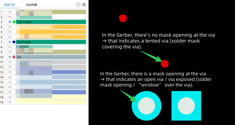
In the Solder Mask Layer, the logic follows a "negative" image format:
When CAM engineers process your order, CAM software reads the Gerber data directly. If there is an opening graphic at that location on the Gerber layer, the equipment will execute the opening. At this point, even if you write "Tent All Vias" ten times in the order remarks, once it enters the automated photoplotting process, the system will faithfully execute the "Open" instruction found in the Gerber.
>> Recommend reading: A Comprehensive Exploration of What Is a Gerber File?
This is not the factory shirking responsibility, but rather to protect your high-level design intent.
For simple consumer electronics boards, tenting the whole board might carry little risk. However, in high-layer-count, high-density, or specialized industry designs, arbitrarily modifying the solder mask is extremely dangerous.
Suppose you designed a power board with Thermal Vias or test holes for In-Circuit Testing (ICT). These vias must be exposed in the Gerber.
If the factory, acting on a generic "Via Tenting" instruction selected during ordering, arbitrarily deleted the opening graphics in the Gerber, the result would be: Thermal failure leading to overheating, or insulated test points making testing impossible.
For R&D teams in rapid iteration or automotive/medical clients with strict traceability requirements, "verbal modification" is a taboo in quality management.
If you request the factory to modify the solder mask via email or phone, but the source file is not updated synchronously, there is a high probability that the old, incorrect Gerber will be used again during the next Re-order or production transfer, leading to batch scrapping.
Conclusion: The factory has no right and should not arbitrarily modify Gerber files that constitute your core intellectual property parameters. "Manufacturing according to the drawing" is the greatest respect for design integrity.
To ensure BGA soldering yield and long-term product reliability, please strictly follow this "Three-Step Method":
In EDA software (Altium, KiCad, Cadence, etc.), do not rely on global output settings, but define them explicitly in the design rules.
Do not just trust the Design View in your EDA software. After exporting to Gerber, you need to use professional CAM tools for a "What You See Is What You Get" inspection.
Here are two highly efficient tools recommended for you, depending on your scenario:
Scenario A: Quick Check & Sharing (Web-based)
If you need to quickly confirm whether the solder mask covers the vias under the BGA, or want to send it to a colleague for review:
>> Use NextPCB Free Online Gerber Viewer Now
No installation required, simply upload the zip package and view the Solder Mask layer layer-by-layer. If there is a graphic, it's exposed; if not, it's tented. Clear at a glance.
Scenario B: Complex Boards & Deep Analysis Before Mass Production (PC-based)
For high-density boards where aperture sizes are too small or hole counts exceed ten thousand, naked-eye inspection can easily miss errors. You need an automated DFM analysis tool:
>> Download NextPCB Desktop DFM Analysis Software
It automatically analyzes Gerber files, detecting open/short circuit risks, overly thin solder mask bridges, and potential via tenting anomalies, simulating the real production pre-audit process.
Ensure that the options (Via Tenting / Via Plugging) in the ordering interface are completely consistent with the actual state of the Gerber file you uploaded. If you find the file is wrong, you must return to the EDA software to modify and re-export it, rather than attempting to correct it through remarks.
Below are frequently asked questions derived from real user searches regarding PCB solder mask and Gerber files.
A: This is a common confusion. The Solder Mask layer defines where the protective ink goes (or rather, where it doesn't go, as it's usually a negative layer). It protects the copper tracks. The Solder Paste layer (or Paste Mask) is used to create the stainless steel stencil for applying solder paste onto SMD pads before reflow. They are not interchangeable.
A: Tenting means covering the via with solder mask ink (the green oil) to insulate it. It is the standard, low-cost method. Plugging (or Via Filling) involves physically filling the via hole with resin or copper, then plating over it (Via-in-Pad). Plugging is required for high-density designs like BGA but is more expensive. Tenting is defined in the Gerber; Plugging usually requires additional fabrication notes.
A: This is called Solder Mask Expansion (or Clearance). It creates a safety margin (typically 2-4 mils) to account for slight misalignments during manufacturing. If the mask opening were the exact same size as the pad, any slight shift might cause the mask to cover part of the pad, affecting solderability.
A: While technically possible using CAM software, it is highly discouraged. Modifying the Gerber breaks the link between your design source (CAD) and the manufacturing data. If you need to re-spin the board later, your manual edits will be lost, leading to errors. Always modify the source design and re-export.
A: You don't need expensive CAM tools. You can use a free online tool like the NextPCB Gerber Viewer. Simply upload your zip file and look at the Solder Mask layer. If you see holes or circles over your vias on this layer, they are exposed. If the area over the via is blank (solid color matching the rest of the mask), they are tented.
In PCB manufacturing, every tiny parameter can determine the life or death of a product. For engineers pursuing extreme performance and reliability, the Gerber file is not just production data, but a legal declaration of your design intent.
NextPCB is dedicated to being your most trustworthy manufacturing partner. While we perform standard CAM audits upon receiving files, for the sake of your project schedule and yield, "Consistency between Gerber and Requirements" is always the most efficient pass.
Unsure if your Gerber meets production standards?
Upload your files to our NextPCB DFM System for a pre-audit run to intercept hazards before production, saving you valuable R&D time and costs.

Still, need help? Contact Us: support@nextpcb.com
Need a PCB or PCBA quote? Quote now

