

 NextPCB Capabilities
 PCB Assembly
 Layer Buildup
 SMD-Stencils
 PCB Design-Aid & Layout
 Mechanics
 Surface
 Quality
 Drills & Throughplating
 Factory & Certificate


Definition: Rigid PCB assembly mounts and solders electronic components onto a rigid printed circuit board (PCB). These boards use solid, inflexible materials such as FR-4 or glass-reinforced epoxy laminates.
Before assembly, the board is simply a rigid PCB. After components are installed and soldered, it becomes part of a PCBA (Printed Circuit Board Assembly).
Rigid PCB assembly is one type of PCBA. PCBA covers all PCB types—rigid, flexible, and rigid-flex. Rigid PCBs are the most common in consumer electronics, automotive, industrial control, aerospace, and medical devices. They offer high strength, dimensional stability, and cost efficiency.

The manufacturing process for rigid PCB assembly mainly uses two methods among all PCBA capabilities: Through-Hole Technology (THT) and Surface Mount Technology (SMT). SMT dominates high-density, automated production. THT remains vital for large, high-power, or mechanically stressed parts.
Many designs use a hybrid assembly of THT and SMT. Others use only full-surface SMT. The method depends on component type, circuit complexity, mechanical needs, and the facility's capabilities.
1. Design & Documentation
Bill of Materials (BOM):
- A/B class: Chips with life cycle tracking
- C class: Grouped passive components
- D class: Mechanical parts with 3D models
Click to get BOM Services from NextPCB.
Placement file setup:
- IPC-D356A format with clear polarity markings
- Corrected part rotation (±0.15°)
Solder stencil design:
- 15° angled openings for tiny BGA chips
- Special coatings ensuring >95% paste transfer
Testing preparation:
- 0.8mm test points covering >92% connections
- Boundary scan connections for advanced FPGAs
2. Assembly Process Overview
Step 1: Solder Paste Stenciling
Before component placement, solder paste must be precisely deposited onto the designated component pad areas of the bare PCB. This gray-colored paste is typically applied using a stencil overlying the board, ensuring position and volume accuracy essential for Surface Mount Technology (SMT). Following application, manufacturers often perform Solder Paste Inspection (SPI) to verify deposit quality before proceeding.
Step 2: Placing Components
High-precision pick-and-place machines automate the placement of standard Surface Mount Devices (SMDs) onto the solder-pasted PCB. Components designated as non-washable or particularly sensitive are usually placed during this stage or handled separately later to avoid subsequent cleaning processes.
Step 3: Reflow Soldering
Reflow soldering creates the permanent electrical connections between components and the board. Loaded onto a conveyor, the populated PCB travels through a reflow oven. Heaters within the oven melt the solder paste according to a carefully controlled thermal profile involving preheat, soak, reflow peak, and controlled cooling phases.
This melts the solder then solidifies it, forming strong, reliable solder joints without thermal damage to components.
Step 4: Waving Soldering
If the PCB design includes through-hole components (PTH/THT), wave soldering connects them. A conveyor transports the board over a standing wave or series of waves of molten solder. As the board passes, solder effectively flows into the plated through-holes, bonding component leads to pads/vias and forming robust electrical connections.
Alternatives to conventional wave soldering include manual or selective soldering, chosen based on design complexity and production volume.
Recommend Reading: Reflow Soldering and Wave Soldering: Difference and Process
Step 5: Cleaning
Post-assembly cleaning removes flux residues and contaminants using deionized (DI) water, isopropyl alcohol (IPA), or dedicated cleaning agents. This critical step enhances reliability and prepares surfaces for subsequent processes like conformal coating. Even assemblies employing "No-Clean" flux often undergo cleaning to improve coating adhesion.
Cleaning can alternatively occur after final inspection.
Step 6: Soldering Non-Washable/Delicate Components
Specific delicate components incompatible with the standard cleaning chemistry (e.g., some MEMS sensors) are finalized after the cleaning step. This typically employs "No-Clean" solder paste and precise techniques like hand soldering or selective soldering.
Step 7: Inspection and Functional Testing
Comprehensive inspection identifies defects such as misaligned components, poor solder joints, opens, or shorts which might occur during processing. Testing uses methods such as Manual Visual Inspection (MVI), Automated Optical Inspection (AOI), and X-ray inspection. X-ray inspection helps find hidden joints and BGAs.
Finally, electrical functional testing checks that everything works correctly. It uses methods like In-Circuit Test (ICT) or Flying Probe Test. These methods validate the assembled PCB's functionality before delivery.
Step 8: Optional Conformal Coating
For boards used in tough environments like moisture, dust, and chemicals, a conformal coating is important. This coating can be acrylic, silicone, or urethane. It helps protect the boards effectively.
Step 9: Packaging and Delivery Preparation
Fully assembled, inspected, tested, and optionally coated PCBs receive final ESD and moisture-resistant packaging according to required specifications before shipment.
3. Component Sourcing & Turnkey Services
|
Module |
Technical Execution |
Risk Mitigation |
|
Global Sourcing |
API integration with 18 distributors |
Component lifecycle mapping dashboard |
|
Alternate Source Eng. |
Parametric matching engine (>20k components) |
48-hour cross-reference validation |
|
Turnkey Integration |
Single-point control from Gerber to shipment |
Live production tracking portal |
|
OBS Management |
6-month safety stock for EOL items |
Counterfeit detection via XRF/decapsulation |
Visit HQ Oline for Electronic Components at Competitive Prices
4. Manufacturing Capabilities & Technical Certifications
In the field of rigid PCB assembly, advanced manufacturing capabilities work hand in hand with strict quality controls to ensure boards meet both functional and reliability requirements.
4.1 Advanced PCB Processing
Fine circuit technology makes it possible to create very narrow 3 µm traces with equal spacing. This is important for making dense, high-performance layouts.
You can drill and plate micro-vias as small as 50 µm. This helps create complex multi-layer connections in rigid PCB assembly.
For power-heavy designs, you can use heavy copper options. These options include up to 6-ounce inner layers with ±8% thickness control. This ensures great current-carrying capacity and thermal stability. Furthermore, precision copper core cutting techniques are applied to enhance heat dissipation, which is critical in high-power rigid PCBs.
Moreover, a wide selection of specialty materials supports application-specific needs. Rogers 4350B laminates are used in high-frequency rigid PCB designs over 18 GHz. They provide low dielectric loss and stable electrical performance. Similarly, aluminum-based rigid boards are provided, delivering superior heat management for LED lighting, automotive electronics, and industrial control systems.
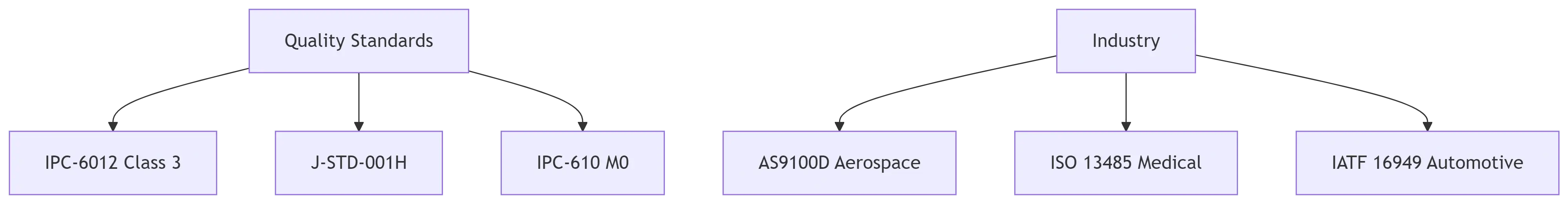
4.2 Quality Approvals
To guarantee consistent performance, every rigid PCB assembly project follows internationally recognized quality benchmarks. This includes full compliance with IPC Class 2 and Class 3 standards for commercial, industrial, and high-reliability products. In addition, the facility holds ISO 13485 certification for medical device manufacturing and AS9100 for aerospace quality systems. Finally, RoHS compliance ensures environmentally responsible production, creating a complete ecosystem where quality, reliability, and sustainability align.
See NextPCB's Quality Certifications and Test Reports
5. Industry Application Engineering & Value Metrics
|
Sector |
Critical Implementation |
ROI Impact |
Reliability Validation |
|
Automotive |
3D-MID integration |
ECU weight ↓35% |
AEC-Q100 Grade 2 |
|
Medical |
Class III biocompatible coating |
Sterile cycle ↑3× longevity |
IEC 60601-1 ESD immunity |
|
Aerospace |
Rad-hard component integration |
SWaP-C ↓40% |
MIL-STD-883 TM2012 |
|
Industrial |
IP68-rated thermal management |
MTBF >400k hours |
UL HazLoc certification |
6. Verification Stages in PCB Assembly
To ensure every PCBA meets high-quality standards, the process includes multiple verification stages. These stages are designed to detect and prevent defects before boards are shipped to customers.

Zero-Defect Manufacturing Framework
Stage 1: Manufacturing Controls
During production, we carefully monitor the application of solder paste. This helps us achieve placement accuracy within ±10 µm.
This ensures that the solder joints are reliable. Technicians use low-oxygen soldering environments (<50 ppm) to minimize oxidation and prevent joint defects.
Automated Optical Inspection (AOI) systems scan the boards. They can find over 500 types of faults. These include misalignments, bridging, and not enough solder.
Stage 2: Failure Investigation
If any defects are identified, a detailed failure investigation is carried out. Cross-sectioning allows engineers to examine the internal connections within the board, ensuring structural integrity. Researchers use high-powered microscopes to look for solder voids and other tiny problems. These issues can affect long-term performance.
By following these thorough verification steps, we make PCB assemblies that meet high performance and reliability standards. This helps reduce the risk of defects in the final product.
7. Summary of Rigid PCB Assembly Advantages and Applications
|
Advantage |
Key Feature |
Benefit in Rigid PCB Assembly |
Typical Applications |
|
Strong base material |
Glass-reinforced epoxy (FR-4/FR-5) |
Secure component mounting, supports heatsinks and connectors handling >5W heat |
Power electronics, industrial controllers |
|
Heat resistance |
Tg 150–180°C |
Maintains shape during 260°C lead-free soldering, ideal for multi-layer boards |
Automotive ECUs, aerospace modules |
|
Fast production |
Placement speed >75,000 pcs/hour (0201 components) |
High efficiency; fixtures enable double-sided soldering |
Consumer electronics, communication devices |
|
Stable signals |
Dk/Df control ±0.02 |
Consistent electrical performance, even for 30-layer boards with 2/2mil circuits |
High-speed networking, server motherboards |
|
Cost-effective manufacturing |
Large 21″×30″ panels, thin 0.005″ boards |
>98% production yield, reduced cost per unit |
Mass-produced industrial PCBs, IoT devices |
Conclusion
Rigid PCB assembly delivers high durability, thermal stability, and signal integrity, making it ideal for industries from consumer electronics to aerospace. Combining advanced manufacturing, strict quality control, and IPC-compliant processes achieves reliable, high-performance boards.
NextPCB provides complete rigid PCB assembly. They handle everything from design checks to perfect production. This helps lower costs and speed up time to market.

