
 NextPCB Capabilities
Printed Circuit Boards
NextPCB Capabilities
Printed Circuit Boards
 PCB Assembly
 Layer Buildup
 SMD-Stencils
 PCB Design-Aid & Layout
 Mechanics
 Quality
 Drills & Throughplating
 Factory & Certificate
 PCB Assembly Factory Show
Certificate
PCB Assembly Factory Show
Certificate
Support Team
Feedback:
support@nextpcb.com


Plated-through-hole (PTH) technology revolutionized the printed circuit board (PCB) industry, making it possible to connect components on opposite sides of a PCB without the need for wires or jumpers. This article traces the evolution of PTH technologies from the early 1950s to the present day.
In the early 1950s, the Motorola Corporation developed the Placir method, which involved sensitizing the surface and hole walls of an unclad panel with SnCl2 and metalizing with silver using a two-gun spray. The panel was then screened with a reverse conductor pattern, plated with copper by electroplating, and finished by removing the silver and resist ink. However, the migration of silver traces underneath the copper conductors was a problem with this method. Around the same time, Fred Pearlstein published a process involving electroless nickel plating for metalizing nonconductive materials, which was applied to making PTHs using copper-clad laminates. But this process was incompatible with the copper surface, leading to the development of better catalysts in the 1960s.
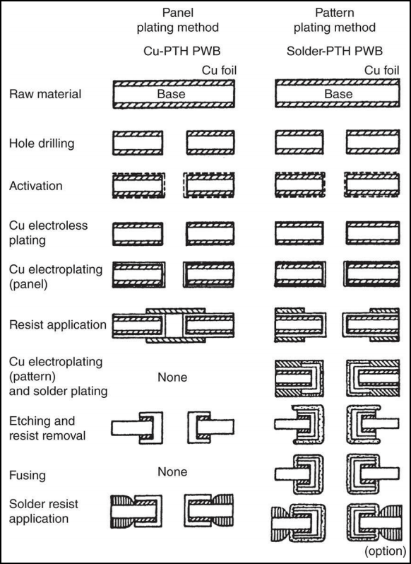
Photocircuits Corporation developed the fully additive PWB manufacturing technology known as the CC-4a process in the 1950s. The modern PTH processes using SnCl2-PdCl2 catalysts and EDTA-base electroless copper-plating solutions were established in the 1960s. The subtractive method, which begins with copper-clad laminates, involves pattern plating and panel plating. In the pattern-plating method, plating resist layers are formed on both sides of the panel. Various steps of electroplating and etching are performed to form the desired conductor pattern. In the panel-plating method, the panel is plated with electrolytic copper, and the holes are filled with ink or covered with dry film before etching.
The pattern-plating method is preferred for boards with fine-line conductors, as it provides better adhesion of dry film and enables padless micro-via holes. However, the current distribution problem is difficult to solve, and solder bridging can occur when the conductor width and clearance are small. The use of ultrathin copper foil offers an advantage in etching, but the process requires constant fine-tuning and maintenance of the hot-air solder coater leveler.
There are some minor variations in the pattern-plating method:
> Recommend reading: PCB Back Drilling (CDD): The Essential Technique for Eliminating Via Stubs in High-Speed PCBs
The panel-plating method is ideal for bare copper boards and is widely used in Japan. However, it is difficult to make the pad less via holes using this method. The conductor width of 0.004 in is considered the minimum realizable by this method for mass production.
The simplified sequence of the panel-plating method is as follows:
The additive process involves electroless copper deposition and can form PTHs solely by this method. There are three basic methods: fully additive, semiadditive, and partially additive. The semiadditive process involves pattern electroplating for PTHs with very thin surface copper, while the other two form PTHs solely by electroless copper deposition. The additive process has various advantages over the subtractive process in forming fine-line conductors and PTHs of a high aspect ratio.
PTH technology has come a long way since the Placir method was developed in the 1950s. Today, PWBs still play an important role in electronic packaging, and the choice of which packaging technology to use is governed by many factors, including cost, electrical requirements, thermal requirements, and density requirements. PTH technologies continue to evolve, and new methods are being developed to address the challenges posed by miniaturization and high-density interconnects.
Still, need help? Contact Us: support@nextpcb.com
Need a PCB or PCBA quote? Quote now


 Surface

