With the development of 5G communications, millimeter-wave radar, satellite communications, automotive electronics, wireless modules, and high-frequency test equipment, RF PCBs (Radio Frequency Printed Circuit Boards) impose higher requirements on PCB manufacturing capability.
Unlike conventional FR-4 PCBs, RF PCBs operate in high-frequency signal environments. Any minor material variation, impedance deviation, copper thickness change, or manufacturing error may result in:
- Increased signal loss (Insertion Loss)
- Impedance mismatch (Impedance Mismatch)
- Signal reflection (Return Loss)
- Phase shift (Phase Shift)
- Reduced antenna efficiency
- Lower system stability
Therefore, RF PCB manufacturing is not merely a matter of "switching materials." It requires coordinated optimization across material selection, PCB design, lamination processes, impedance control, surface finish, and quality inspection.
How to Select RF PCB Materials?
Three Core Electrical Parameters for Material Selection
The selection of RF PCB materials ultimately centers on three key indicators:
- Dielectric Constant (Dk): Determines signal propagation velocity in the medium and the characteristic impedance of traces. Lower Dk reduces propagation delay; Dk stability is equally critical—Dk variation with frequency or temperature can cause impedance drift and signal distortion. For example, in low-frequency designs, a Dk shift from 4.2 to 4.4 may have limited impact, but in millimeter-wave applications, even minor changes can lead to noticeable performance degradation.
- Dissipation Factor (Df): Measures the extent to which signal energy is converted into heat within the substrate. Lower Df results in less signal attenuation and higher transmission quality. Above 10 GHz, small differences in Df are significantly magnified.
- Thermal Stability: Includes glass transition temperature (Tg) and coefficient of thermal expansion (CTE). High-frequency equipment generates substantial heat during operation; insufficient heat resistance of the substrate may lead to deformation, delamination, and other issues.
General guideline:
| Application |
Recommended Material Characteristics |
| General high-speed communication |
Medium-to-low Df materials |
| 5G high-frequency |
Low-loss materials |
| Radar/millimeter-wave |
Ultra-low-loss materials |
Comparison and Selection Guide for Common RF PCB Materials
| Material Type |
Representative Product |
Dk Range |
Df (@10GHz) |
Applicable Frequency |
Cost |
Processing Difficulty |
| Epoxy (FR-4) |
Standard FR-4 |
4.2–4.8 |
0.02–0.03 |
<1 GHz |
Low |
Low |
| PPO/PPE-based |
Modified PPO |
3.0–3.5 |
~0.005 |
1–10 GHz |
Medium |
Medium |
| Hydrocarbon resin + ceramic |
Rogers RO4000 series |
3.38–3.55 |
~0.004 |
≤26 GHz |
Medium-high |
Medium (FR-4 process compatible) |
| PTFE-based |
Rogers RO3000 series / PTFE |
2.0–3.0 |
≤0.002 |
Millimeter-wave (≥30 GHz) |
High |
High |
| Liquid Crystal Polymer (LCP) |
LCP |
2.9–3.2 |
~0.002 |
Millimeter-wave |
High |
Medium-high |
When selecting RF PCB materials, do not focus on price alone. Consider the following:
1) Select by operating frequency
- Frequency < 1 GHz: Modified FR-4 or high-performance epoxy resin can meet the requirements.
- Frequency 1–10 GHz (e.g., 4G/5G base stations, routers): PPO/PPE-based materials are cost-effective options. Rogers RO4000 series is the "gold standard" because it offers strong electrical performance while remaining compatible with FR-4 processing, making it suitable for mass production.
- Frequency > 10 GHz (e.g., 5G mmWave, satellite communications, 77 GHz automotive radar): PTFE-based materials or Rogers RO3000 series are required. PTFE has a low dielectric constant (2.0–2.3) and very low dissipation factor (< 0.001), making it one of the best high-frequency material choices. The RO3000 series uses ceramic-filled PTFE composites, with excellent Dk stability, making it the preferred option for high-end satellite communications and military radar.
2) Select based on cost requirements
In product development, balance cost and performance while adjusting dynamically across the lifecycle. During prototype validation, use high-performance materials (e.g., full-layer Rogers or PTFE) to quickly and aggressively verify performance. In mass production, switch to a "mixed stack-up" strategy: keep high-performance materials only on critical RF signal layers, and use cost-effective FR-4 on non-critical layers such as power and low-speed control. This maintains core performance while optimizing supply chain and material costs to maximize commercial margins.
3) Select based on manufacturing capability
RF PCB material selection is not only a sourcing decision; it depends heavily on the PCB factory's process capability. The factory must have mature experience with high-frequency materials and demonstrate strong manufacturing performance in special via drilling, precise impedance control, and complex lamination parameter management. Only when the design intent and manufacturing process are matched accurately can the product's high-frequency performance be effectively realized.
Selection of copper foil and solder mask
- Copper foil: For high-frequency signals, current tends to concentrate on the conductor surface due to the skin effect, so copper foil surface flatness directly affects signal loss. It is recommended to use low-profile copper (LP) or ultra-low-profile copper (HVLP, Rz ≤ 0.4 μm) to reduce surface roughness and thereby reduce skin-effect losses. In addition, select high-purity copper foil to minimize resistive losses.
- Solder mask: In RF PCBs, the solder mask's dielectric properties cannot be ignored. If the dielectric constant is too high or fluctuates, it can introduce interference to adjacent traces. Choose a solder mask with a low and stable dielectric constant and low dielectric loss.
Process Control: Key Points Across the Full Workflow from Design to Manufacturing
"Selecting the right material is only half the battle"—even the best material will yield significantly degraded high-frequency performance if process control is inadequate.
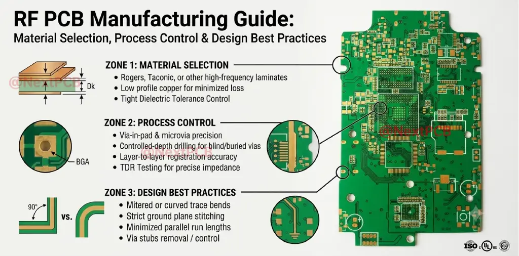
1. Impedance Control
Impedance control is the most critical process requirement in RF PCB manufacturing:
- Trace width/spacing precision: Trace width tolerance must be maintained within ±0.5 mil (approx. ±12.7 μm) to keep impedance within specification. Advanced processes can achieve trace width tolerance within ±5 μm.
- Dielectric thickness control: Minor variations in dielectric layer thickness during lamination directly cause impedance drift.
- Copper thickness control: Copper foil thickness deviation also affects impedance, requiring precise control of plating and etching processes.
- Impedance testing: RF PCBs must undergo 100% inspection using an impedance analyzer (frequency range 1 MHz–40 GHz) to ensure impedance deviation ≤ ±3% (at 28 GHz); differential impedance deviation ≤ ±2%.
2. Etching Process
Etching determines the final dimensions and shape of traces:
- Optimize etchant concentration, temperature, and etching time to control etch rate and depth.
- Employ advanced photolithography and precision etching equipment to ensure trace width consistency and edge smoothness.
- Trace width tolerance should be controlled within ±8% of the designed value (when design value < 0.1 mm).
3. Lamination Process
Lamination of multilayer RF PCBs is a critical step:
- Precisely control lamination temperature, pressure, and time profiles—different materials have varying coefficients of thermal expansion, requiring specific temperature-pressure profiles tailored to material characteristics.
- Ensure precise alignment of each layer; interlayer registration error must be controlled within 10% of the hole diameter.
- Prevent defects such as interlayer voids and delamination.
4. Surface Finish
Due to the skin effect, high-frequency signals are primarily transmitted on the conductor surface; the quality of the surface finish layer directly affects signal integrity:
- ENIG (Electroless Nickel Immersion Gold): Provides a flat and smooth surface; the gold layer offers excellent solderability and conductivity, making it ideal for microwave and RF applications.
- Immersion Silver: Balances performance and cost; provides a flatter surface suitable for very high-frequency signals and effectively reduces losses caused by the skin effect, though oxidation and tarnishing must be prevented.
- Hard Gold: Suitable for high-frequency applications such as contacts and connectors, offering excellent conductivity and wear resistance.
- Immersion Tin: Smooth surface but poor corrosion resistance; less commonly used in RF PCBs.
Key reminder: The thickness and uniformity of the surface finish layer alter the actual conductor dimensions—this effect is minor at low frequencies but significantly impacts impedance at high frequencies.
5. Drilling and Via Control
Vias are a major source of impedance discontinuity in high-frequency signal paths:
- Prioritize back-drilling to remove via stubs.
- Minimize the use of vias in RF paths and avoid layer transitions where possible.
- Optimizing anti-pad diameter is a common method to reduce via impedance discontinuity.
Work that should be done during the design phase
High-frequency performance optimization should not be deferred until the manufacturing stage. Source-level control in the design phase is equally critical:
- Maintain consistent RF trace impedance: Usually 50Ω or 75Ω. Keep trace width and the distance to the reference ground plane constant.
- Keep RF traces as short and as straight as possible: Reduce signal attenuation and parasitic effects.
- Avoid sharp corners: Use 45° chamfering or curved trace routing.
- Separate RF and digital areas: Keep at least a 20 mm spacing to prevent coupling.
- Use a continuous ground plane: A complete ground layer directly under the RF trace is required to ensure a proper return path.
- Perform simulation verification: After finishing the design, use impedance calculation and electromagnetic simulation tools to validate and resolve potential issues early.
Common RF PCB faults and signal integrity problems
RF PCB failures are often not obvious "open" or "short" conditions. Instead, they present as signal degradation and unstable performance. The three most common high-frequency fault types are:
1. Impedance mismatch and signal reflection
Symptoms: overshoot/undershoot, ringing on the waveform, increased return loss, and reduced transmission power.
Root cause: when the transmission line's characteristic impedance does not match the source or load impedance, part of the signal energy reflects back to the source. Contributors to impedance mismatch include:
- inconsistent trace width or variation in distance to the reference plane
- via-induced impedance discontinuities; when frequency > 1 GHz, via effects cannot be ignored
- non-uniform lamination dielectric thickness
- mismatch between the material's actual Dk value and the designed value
Troubleshooting: use a TDR to measure impedance distribution along the trace and locate impedance step points; use a VNA to measure return loss (S11).
2. Crosstalk and EMI (Electromagnetic Interference)
Symptoms: unintended coupling between adjacent signal lines, degraded signal quality, and EMI exceeding system limits.
Root cause: at high frequency, electromagnetic field coupling increases with frequency. Even when trace spacing appears sufficient at 1 GHz, unacceptable crosstalk may occur at 10 GHz. Parallel routing of RF and digital lines, incomplete ground planes, and lack of shielding structures further worsen the issue.
Troubleshooting: scan the PCB surface with a near-field probe to locate interference sources; check spacing and parallel run lengths between adjacent traces.
3. Skin effect and conductor loss
Symptoms: excessive attenuation, reduced transmission distance, and worse signal-to-noise ratio.
Root cause: at high frequency, current concentrates in an extremely thin layer at the conductor surface. The rougher the copper foil surface, the longer the effective current path and the higher the resistance. Studies indicate that copper foil surface roughness Ra=1μm results in approximately 3Ω higher impedance than Ra=0.5μm; insertion loss increases progressively as surface roughness increases.
Troubleshooting: measure insertion loss (S21) versus frequency; use a surface profilometer to measure copper roughness.
4. Other common problems
- poor grounding: ground-plane discontinuities break the return path, causing common-mode radiation and noise
- sharp-angle routing: 90° corners create impedance discontinuities and reflections
- improper via design: via stubs (stub remnants) cause resonance and additional loss
RF PCB Design and Manufacturing – Common Misconception Guide
Misconception 1: Assuming More Expensive Materials Always Deliver Better Performance
- Mistake: Blindly equating high-cost materials with superior performance, and pursuing top-tier RF substrates in all scenarios.
- Reality: Material selection must match the specific application. Over-specifying expensive materials significantly increases project cost and may add manufacturing difficulty due to the complexity of substrate characteristics, while the actual performance gain at a given frequency band or bandwidth requirement is often limited—and may even result in performance degradation due to mismatch.
Misconception 2: Focusing Only on PCB Materials While Ignoring Manufacturing Capability
- Mistake: Believing that RF PCB performance is entirely determined by the material datasheet parameters, disregarding the production process.
- Reality: The final performance of an RF PCB is the product of "material, design, and manufacturing" combined. Even with top-grade materials, if the PCB fabricator lacks proven high-frequency processing experience and cannot precisely control special drilling, impedance control, and lamination parameters, the finished board may still exhibit severe performance degradation or out-of-spec indicators.
Misconception 3: Neglecting the Accuracy of Gerber Files and Manufacturing Data
- Mistake: Assuming that RF board manufacturing data is no different from standard PCBs, and that providing simple Gerber files meets delivery standards.
- Reality: RF PCBs have stringent requirements for manufacturing data completeness. In addition to standard Gerber files, complete stackup information, impedance requirements, material type, copper thickness, and other critical process parameters must be clearly specified. For complex high-frequency circuits, it is advisable to use integrated data formats such as ODB++ or IPC-2581 to minimize ambiguity in production communication and reduce the risk of manufacturing misinterpretation.
How to Select a Reliable RF PCB Manufacturer
Selecting a reliable RF PCB manufacturer is a core guarantee for successful RF design implementation. When evaluating an RF PCB manufacturer, the following aspects are recommended:
- Material Processing Expertise: Verify that the factory has proven experience in high-frequency material processing, particularly with industry-standard materials such as Rogers, Taconic, and Panasonic Megtron—including lamination and processing proficiency. This directly determines the fundamental assurance of signal integrity.
- Precision Impedance Control: RF performance is highly dependent on impedance matching. Suppliers must be able to provide professional impedance control solutions and deliver detailed TDR (Time-Domain Reflectometry) test reports with each shipment, ensuring that the characteristic impedance of the fabricated board meets design simulation expectations.
- Industry Track Record: Examine the manufacturer's past project portfolio. Priority should be given to suppliers with deep experience in automotive millimeter-wave radar, high-speed communication base stations, and similar applications. Such applications demand high reliability and consistency; the manufacturer's industry experience is key to mitigating mass-production risks.
- Agile Engineering Support: RF development typically involves multiple design iterations. A reliable partner should not only support quick-turn prototyping but also have a robust engineering feedback mechanism to assist in optimizing production solutions during small-batch pilot runs, helping shorten the product development cycle.
Beyond the core criteria above, professional RF PCB fabrication is further distinguished by:
- Manufacturing Tolerances: Inquire about their capabilities regarding trace width, spacing, and registration accuracy. Even minor deviations in etching or layer alignment can shift the resonant frequency or cause significant impedance discontinuities.
- Surface Finish Quality: High-frequency performance is susceptible to surface finish effects. Discuss options like ENIG (Electroless Nickel Immersion Gold) or Immersion Silver, and ensure the supplier can maintain the required surface roughness specifications to minimize conductor loss.
- Quality Management Systems: Ensure the facility holds relevant certifications (e.g., ISO 9001, IATF 16949 for automotive) and has the internal capability to perform cross-section analysis and thermal shock testing to validate board durability.
Conclusion
High-frequency performance optimization for RF PCBs is a system engineering effort spanning materials and process control. Selecting the right material is the foundation—choose correctly among FR-4, PPO, Rogers RO4000/RO3000, PTFE, and others based on operating frequency. Strict process control is the guarantee—every step, from impedance control, etching accuracy to lamination and surface finishing, directly affects final performance. Design optimization is the prerequisite—reasonable layout, routing, and grounding strategies fundamentally reduce signal integrity issues.
In today's increasingly competitive high-frequency electronic equipment market, only by integrating materials science, manufacturing processes, and design methodology can RF PCB products achieve true high performance and high reliability.
Upload Files, Get RF PCB Price
RF PCB – Frequently Asked Questions
Q1: What is an RF PCB, and how is it different from a standard PCB?
A: An RF PCB (Radio Frequency Printed Circuit Board) is designed to handle high-frequency signals, typically above 1 GHz. Unlike standard FR-4 PCBs, RF PCBs require strict control over material properties (Dk, Df), impedance matching, and manufacturing precision to minimize signal loss, reflection, and distortion.
Q2: How do I choose the right RF PCB manufacturer?
A: Look for a manufacturer with proven experience in high-frequency materials (e.g., Rogers, Taconic, PTFE), precision impedance control with TDR testing, a strong track record in automotive radar or telecom applications, and agile engineering support for quick-turn prototyping and design iteration.
Q3: What materials are commonly used for RF PCBs, and how do I select them?
A: Common materials include FR-4 (<1 GHz), PPO/PPE-based (1–10 GHz), Rogers RO4000 series (≤26 GHz), PTFE/RO3000 (millimeter-wave), and LCP. Selection depends on operating frequency, cost budget, and manufacturing capability—higher frequency generally requires lower Dk and Df materials.
Q4: Why is impedance control so critical in RF PCB manufacturing?
A: Impedance mismatch causes signal reflection, increased return loss, and reduced transmission power. RF PCBs require tight trace width tolerances (±0.5 mil or better), precise dielectric thickness control, and 100% impedance testing to ensure deviation stays within ±3% at high frequencies.
Q5: What are the most common signal integrity issues in RF PCBs?
A: The three most common issues are:
- Impedance mismatch – caused by inconsistent trace width, via discontinuities, or non-uniform lamination
- Crosstalk and EMI – caused by insufficient spacing between RF and digital lines or incomplete ground planes
- Skin effect and conductor loss – caused by rough copper foil surfaces increasing resistance at high frequencies
Q6: Can I use standard FR-4 materials for RF applications?
A: FR-4 is suitable only for frequencies below 1 GHz. For higher frequencies (1–10 GHz and above), low-loss materials like PPO, Rogers RO4000, or PTFE are required to maintain signal integrity and minimize attenuation.
Q7: What surface finish is best for RF PCBs?
A: ENIG (Electroless Nickel Immersion Gold) and Immersion Silver are the most common choices. ENIG offers excellent solderability and flatness, while Immersion Silver provides lower loss at high frequencies. The choice depends on performance requirements and cost considerations.
Q8: Why is via design important in RF PCBs?
A: Vias introduce impedance discontinuities that can degrade signal quality at high frequencies. Best practices include back-drilling to remove via stubs, minimizing the number of vias in RF signal paths, and optimizing anti-pad diameters to reduce parasitic effects.
Q9: What should I include in my manufacturing data package for an RF PCB?
A: Beyond standard Gerber files, you must provide complete stackup information, impedance requirements, material types, copper thickness specifications, and surface finish details. Using ODB++ or IPC-2581 formats can reduce communication errors and manufacturing misinterpretation.
Q10: What are the common misconceptions when designing RF PCBs?
A: Three common misconceptions are:
- More expensive materials always deliver better performance – reality: material must match the specific application.
- Focusing only on material selection while ignoring manufacturing capability – reality: performance depends on material, design, and process combined.
- Gerber files alone are sufficient for RF board production – reality: complete manufacturing data is essential for successful fabrication.

 NextPCB Capabilities
 PCB Assembly
 Layer Buildup
 SMD-Stencils
 PCB Design-Aid & Layout
 Mechanics
 Quality
 Drills & Throughplating
 Factory & Certificate
 PCB Assembly Factory Show
Certificate
PCB Assembly Factory Show
Certificate


 Surface

