NextPCB Capabilities
 PCB Assembly
 Layer Buildup
 SMD-Stencils
 PCB Design-Aid & Layout
 Mechanics
 Quality
 Drills & Throughplating
 Factory & Certificate





High-Frequency Mixed-Press Multilayer PCB Delamination Failure Analysis: Root Causes and Fixes for Rogers/FR4 Via-Hole Blistering
As 5G base stations, satellite communications, and other applications continue to demand higher bandwidth and lower latency, communications-grade PCBs are increasingly shifting toward high-speed, high-frequency materials. But high-frequency laminates such as Rogers differ significantly from FR4 in coefficient of thermal expansion, resin system, and surface energy. In Rogers/FR4 mixed-press multilayer boards, via-hole delamination and blistering during SMT assembly are a recurring failure mode. This article walks through the analysis path from a real-world failure case to outline how to identify the root cause of delamination in mixed-press boards and what process improvements actually move the needle, for PCB manufacturing and quality engineers.
1. The Problem
An 8-layer board mixing Rogers 4350B and FR4 developed batch via-hole blistering on its very first pass through lead-free reflow after SMT placement, with a defect rate of roughly 10%. The failures clustered around 4.65mm drilled holes on the Rogers side, affected both large and densely packed small holes, and the blistering locations did not follow any obvious pattern. This pointed toward a problem rooted in interfacial bond strength or micro-damage introduced during processing, rather than simple thermal stress from soldering.
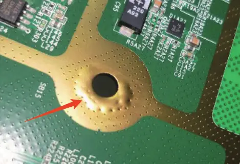
Photo placeholder — replace with your own product photo. Referenced case photo source: An Wei & Zeng Fulin, Fundamentals of PCB Technology for Communication Products and Their Applications (2021).
2. Diagnosing the Failure Mechanism
2.1 Peel Strength Testing: Is the Base Bond Strength Adequate?
As a baseline check, standard peel strength tests were run separately on the large copper foil area and the patterned circuit area. Results came in above the industry threshold of 0.70 N/mm in both cases, indicating the overall copper-to-substrate bond strength was within spec as shipped. In other words, this was not a case of "inherently bad material" — the problem was more likely accumulating damage introduced by downstream processing steps.
| Test Item | Reading 1 | Reading 2 | Reading 3 | Requirement | Result |
|---|---|---|---|---|---|
| Large copper foil area | 0.96 N/mm | 0.93 N/mm | 0.98 N/mm | ≥0.70 N/mm | Pass |
| Patterned circuit area | 1.11 N/mm | 1.07 N/mm | 1.18 N/mm | ≥0.70 N/mm |
2.2 Cross-Section Analysis: Where Exactly Is the Blister Forming?
Cross-section samples were taken from both blistered and non-blistered areas, which revealed two key findings:
- At sites that had already blistered, the separation plane sat at the interface between the base copper and the Rogers bonding layer — meaning the bond layer between the copper foil and the Rogers substrate was the weak point.
- At sites near the hole that had not yet blistered, a similar slight separation between the bond layer and copper foil was already visible, and nickel could be seen migrating into the copper layer at the edge of the plated hole wall.
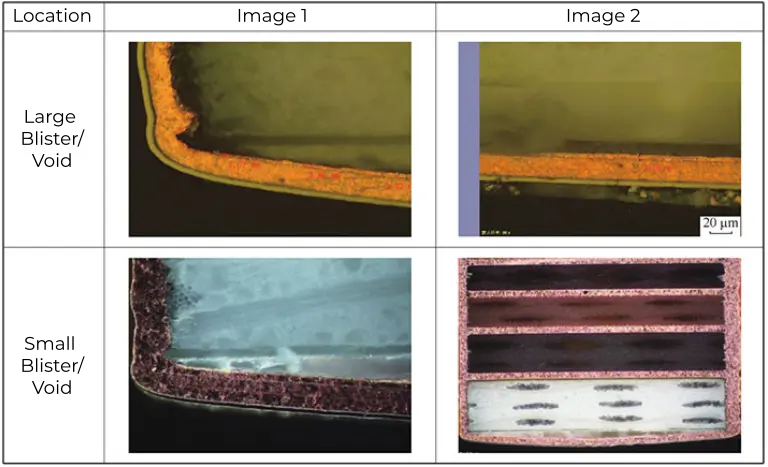
Photo placeholder — replace with your own cross-section/microscopy images. Referenced case photo source: An Wei & Zeng Fulin, Fundamentals of PCB Technology for Communication Products and Their Applications (2021).
This tells us the blistering wasn't a sudden event triggered by reflow — micro-damage at the bond layer/copper foil interface had already occurred earlier in processing, and the high temperature of reflow simply turned an existing latent defect into a visible one. The exposed separation plane at the bond layer suggests the bond layer itself may have accumulated damage from a combination of mechanical impact, thermal cycling, and chemical attack across drilling, grinding, and wet-process steps.
>> Suspect a similar issue on your own design? NextPCB's free HQDFM analysis tool flags via-hole spacing and material-transition risks like the ones described above before your board goes to fab — no quote request required.
3. Pinpointing Risk in the Process Flow
Breaking down the full multilayer fabrication sequence (inner layer → oxide treatment → lamination → ceramic-brush scrubbing → copper reduction → drilling → deburring → routing → desmear → plasma treatment → desmear/etch-back → vertical copper deposition → panel plating → outer-layer imaging) makes it possible to assess which steps are most likely to weaken the bond on the Rogers side:
- Lamination: the high-pressure, high-temperature process itself can reduce the bond strength between the bonding layer and base copper.
- Drilling: mechanical drilling directly shocks the material around the hole, which can create a weak-bond zone near the hole.
- Ceramic-brush scrubbing/deburring: aggressive mechanical brushing of the copper surface can, counterintuitively, weaken the bond-layer-to-copper-foil interface.
- Desmear/vertical copper deposition: the chemistry used in copper deposition attacks both the substrate-to-bond-layer and bond-layer-to-copper-foil interfaces simultaneously. This step — especially given the longer dwell time on vertical deposition lines — deserves close attention.
4. Designing the DOE (Design of Experiments)
To isolate which of these suspected factors was actually driving the failure, a multi-factor comparison test was designed around the following core variables:
- Board thickness: 0.51mm vs. 0.271mm Rogers material.
- Drilling parameters: drill bit wear (new bit vs. 2 uses), spindle speed (±20%), and feed rate (±20%).
- Hole-wall spacing: dense hole arrays at 0.6mm, 0.8mm, and 1.0mm pitch.
- Deburring: performed vs. skipped.
- Plasma treatment: performed vs. skipped.
- Copper deposition line type: horizontal vs. vertical.
Using 0.51mm and 0.271mm boards under normal processing parameters as the baseline, every other run changed a single variable at a time. Each test board was cross-sectioned both before and after reflow to compare blistering behavior across runs and back out how much each factor actually contributed to delamination. A total of 22 test runs were designed, detailed below:
| Run | Thickness (mm) | Drill Wear | Speed | Feed Rate | Hole Spacing (mm) | Deburr | Plasma | Cu Deposition | Purpose |
|---|---|---|---|---|---|---|---|---|---|
| 1 | 0.51 | New | Normal | Normal | 0.8 | Yes | Yes | Vertical | Baseline — confirm delamination behavior across board thicknesses |
| 2 | 0.271 | New | Normal | Normal | 0.8 | Yes | Yes | Vertical | |
| 3 | 0.51 | 2 uses | Normal | Normal | 0.8 | Yes | Yes | Vertical | Correlate delamination with drill bit wear |
| 4 | 0.271 | 2 uses | Normal | Normal | 0.8 | Yes | Yes | Vertical | |
| 5 | 0.51 | New | +20% | Normal | 0.8 | Yes | Yes | Vertical | Correlate delamination with drilling speed |
| 6 | 0.271 | New | +20% | Normal | 0.8 | Yes | Yes | Vertical | |
| 7 | 0.51 | New | -20% | Normal | 0.8 | Yes | Yes | Vertical | |
| 8 | 0.271 | New | -20% | Normal | 0.8 | Yes | Yes | Vertical | |
| 9 | 0.51 | New | Normal | +20% | 0.8 | Yes | Yes | Vertical | Correlate delamination with feed rate |
| 10 | 0.271 | New | Normal | +20% | 0.8 | Yes | Yes | Vertical | |
| 11 | 0.51 | New | Normal | -20% | 0.8 | Yes | Yes | Vertical | |
| 12 | 0.271 | New | Normal | -20% | 0.8 | Yes | Yes | Vertical | |
| 13 | 0.51 | New | Normal | Normal | 0.6 | Yes | Yes | Vertical | Correlate delamination with dense-hole spacing |
| 14 | 0.271 | New | Normal | Normal | 0.6 | Yes | Yes | Vertical | |
| 15 | 0.51 | New | Normal | Normal | 1.0 | Yes | Yes | Vertical | |
| 16 | 0.271 | New | Normal | Normal | 1.0 | Yes | Yes | Vertical | |
| 17 | 0.51 | New | Normal | Normal | 0.8 | No | Yes | Vertical | Correlate delamination with deburring |
| 18 | 0.271 | New | Normal | Normal | 0.8 | No | Yes | Vertical | |
| 19 | 0.51 | New | Normal | Normal | 0.8 | Yes | No | Vertical | Correlate delamination with plasma treatment |
| 20 | 0.271 | New | Normal | Normal | 0.8 | Yes | No | Vertical | |
| 21 | 0.51 | New | Normal | Normal | 0.8 | Yes | Yes | Horizontal | Correlate delamination with copper deposition chemistry |
| 22 | 0.271 | New | Normal | Normal | 0.8 | Yes | Yes | Horizontal |
5. Key Findings
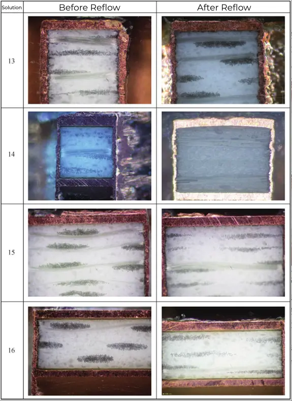
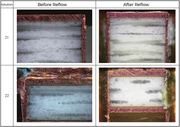
Photo placeholder — replace with your own before/after cross-section images. Referenced case photo source: An Wei & Zeng Fulin, Fundamentals of PCB Technology for Communication Products and Their Applications (2021).
Taken together, the cross-section results from all test runs point to three findings with real engineering value:
- Drill bit wear, spindle speed, feed rate, deburring, and plasma treatment all had negligible impact on Rogers delamination. That means fine-tuning drilling or deburring parameters alone is unlikely to solve this class of delamination problem — attention needs to go elsewhere.
- Hole-wall spacing and copper deposition chemistry had a clear, measurable impact. Tighter hole-wall spacing made delamination more likely — the combined mechanical shock from adjacent holes on the wall and copper layer compounds as spacing shrinks. On the deposition side, horizontal copper deposition lines lowered delamination risk compared to vertical lines. The reason: vertical deposition lines typically have several times longer dwell time in the desmear and swell tanks than horizontal lines, exposing the copper-to-resin bond interface to chemical attack for longer and making delamination more likely.
- Thinner boards (0.27mm) delaminated far more readily than thicker ones (0.51mm). Across every comparison run, blistering and delamination showed up almost exclusively on the 0.27mm Rogers material. That points to board thickness itself as the underlying background factor driving blistering and delamination — thinner boards carry more processing stress and chemical exposure per unit area, leaving less margin at the bond interface.
>> These findings shape how NextPCB engineers Rogers/FR4 mixed-press stackups internally — from hole-wall spacing rules to copper deposition line selection. See our high-frequency PCB manufacturing capabilities for material options and design guidelines we apply by default.
6. Practical Recommendations for Production
- During DFM review of Rogers/FR4 mixed-press boards, allow wider hole-wall spacing for thin (≤0.3mm-class) Rogers layers, particularly in dense hole arrays.
- Prioritize horizontal copper deposition lines for high-frequency mixed-press boards, or evaluate shortening desmear/swell dwell time on vertical deposition lines specifically for this application.
- A passing peel strength test does not mean the process flow is risk-free — add cross-section sampling checks at critical via locations, especially dense hole and large-hole regions, as a supplement to routine peel strength testing.
- For high-frequency, high-speed products, delamination risk on thinner Rogers layers should be evaluated during structural design and material selection, not discovered only after a batch failure.
>> Working on a Rogers/FR4 mixed-press design?
Send us your stackup and via layout — our engineering team will flag delamination risk factors like the ones above before you commit to fabrication.
Get a Quote Browse Our Advanced PCB Manufacturing Capabilities Talk to a PCB Engineer
FAQ
Why are Rogers/FR4 mixed-press boards more prone to via-hole delamination than pure FR4 boards?
Rogers material and FR4 differ in coefficient of thermal expansion, resin chemistry, and surface energy, making the interfacial bond more sensitive to begin with. Layered on top of that, drilling, desmear, and copper deposition all impose mechanical and chemical stress on the via-hole area, which can create weak bond points around the hole. The high temperature of reflow soldering then turns these latent defects into visible blistering and delamination.
If peel strength testing passes, does that rule out delamination risk?
Not entirely. Peel strength reflects the overall macro-level bond between copper foil and the base material across the panel, but delamination tends to occur at localized stress-concentration points such as via holes. These local weak points are not always captured by a panel-level peel strength test, so cross-section analysis is needed for local verification.
How can delamination risk be reduced when designing with thin Rogers material?
It helps to widen the hole-wall spacing in densely packed via areas, prioritize horizontal copper deposition lines over vertical ones, and add cross-section sampling checks specifically for thin-board via areas during process validation, rather than relying solely on panel-level peel strength as the only indicator.
Reference
The photography referenced in this analysis are drawn from: An Wei, Zeng Fulin (eds.), Fundamentals of PCB Technology for Communication Products and Their Applications, People's Posts and Telecommunications Press, 2021.