
 NextPCB Capabilities
Printed Circuit Boards
NextPCB Capabilities
Printed Circuit Boards
 PCB Assembly
 Layer Buildup
 SMD-Stencils
 PCB Design-Aid & Layout
 Mechanics
 Quality
 Drills & Throughplating
 Factory & Certificate
 PCB Assembly Factory Show
Certificate
PCB Assembly Factory Show
Certificate
Support Team
Feedback:
support@nextpcb.com


As 5G, radar systems, and AI computing platforms advance into the GHz and millimeter-wave eras, PCB traces are no longer mere "connecting wires" but critical RF structures that determine system performance. RF circuit design is no longer just simple component stacking; the PCB traces themselves are core components of the circuit's functionality. In High-Frequency PCB and High-Speed PCB design, when signal frequencies or edge rates reach a certain threshold, interconnects must be treated as transmission lines. Starting from physical routing guidelines, this article delves into how to achieve high-performance impedance control through precise stackup planning and Design for Manufacturing (DFM).
In RF circuits, PCB traces typically exist in the form of microstrips or striplines. The impact of these traces on circuit performance often exceeds that of discrete components like capacitors, inductors, or resistors.
In PCB design, the quarter-wavelength (λ/4) is a critical threshold parameter. When the trace length approaches or exceeds 1/4 of the signal wavelength (λ/4), its transmission line effects are significantly amplified. Under specific boundary conditions (such as open or short-circuit terminations), phenomena like impedance inversion may occur. For example, a trace could shift from a short-circuit state to an open-circuit state, or its impedance could abruptly change from zero to infinity.
Therefore, the primary rule in RF layout is to keep traces as short as possible. If the trace length is equivalent to or greater than λ/4, it must be modeled as an independent distributed-parameter component during circuit simulation. By shortening the physical distance, signal attenuation can be effectively reduced, and external electromagnetic interference coupling can be minimized. During layout, RF components should ideally be placed on the same layer to avoid parasitic inductance caused by via transitions.
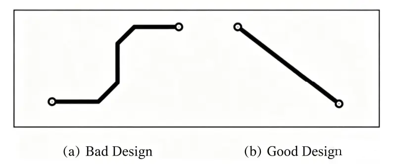
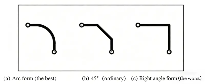
The corner design of RF traces directly affects signal radiation and reflection. Sharp corners (such as 90° right angles) generate singularities in the electromagnetic field, resulting in substantial radiation loss and causing impedance discontinuities due to local trace width variations at the corner.
Experimental data and practical engineering experience demonstrate that smooth, arc-shaped corners are the optimal choice for RF design. Compared to 45° chamfers or right angles, arc connections maximize the continuity of the electromagnetic field and provide the shortest electrical connection path. Maintaining smooth corners is the physical foundation for reducing return loss.
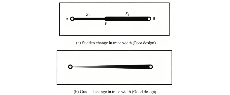
The characteristic impedance of a microstrip line depends directly on its width, dielectric thickness, and dielectric constant. When the trace width changes abruptly (for instance, when transitioning from a wide transmission line to a small IC package pad), that specific point forms an impedance transformer.
This abrupt shift causes RF power to reflect at the transition point and can trigger severe signal radiation. To prevent such catastrophic consequences, designers should employ a tapered trace design to ensure a smooth transition in trace width. This gradual physical transformation guarantees impedance continuity along the transmission path, thereby reducing additional reflection and radiation to acceptable levels.
In RF PCB design, unrelated traces on adjacent or identical layers should be kept orthogonal to each other as much as possible to minimize magnetic field coupling. If parallel routing is unavoidable, a common rule of thumb is the 3W rule (spacing ≥ 3 × trace width). However, in GHz RF designs, it is usually necessary to further increase the spacing based on simulations to meet crosstalk specifications. For sensitive lines transmitting high-frequency signals, increasing the spacing is an essential measure to reduce crosstalk and improve the system's signal-to-noise ratio.
Adhering to the aforementioned physical routing rules is a necessary condition for successful RF design, but it is not sufficient on its own. As frequencies enter the GHz range, the impact of the PCB manufacturing process on impedance becomes impossible to ignore. At this stage, designers must transition from pure electrical design to DFM (Design for Manufacturing).
In high-performance computing (HPC) and RF systems, impedance control is a technical prerequisite. Designers must not only concern themselves with theoretical values in EDA software but also consider the actual performance on the manufacturing end.
Loss budget management in high-frequency circuits begins with material selection. High-frequency losses primarily include conductor loss (skin effect) and dielectric loss, and material selection must account for both factors. Standard FR-4 exhibits high loss and limited dielectric constant stability in the GHz high-frequency band, making it generally inadequate for the stringent loss and consistency requirements of high-performance RF applications. Designers typically need to pre-select special high-Tg, low-loss materials, such as Rogers series or PTFE (Polytetrafluoroethylene) substrates. During the early stages of a project, consulting manufacturers like NextPCB regarding the inventory status and process parameters of these specialized materials is crucial, as the actual Dk (dielectric constant) value of the material will slightly shift depending on the frequency and production batch.
During PCB production, the final thickness of the prepreg after pressing will deviate from the initial specifications due to resin flow. This thickness variation directly affects the accuracy of the controlled impedance.
Therefore, before placing an order, designers should request a recommended Impedance Control & Stackups plan from the factory based on their actual production line processes. Using calculation software (such as Polar SI9000), the factory will combine the actual pressed dielectric thickness, copper thickness, and solder mask coverage to determine the precise trace width required to achieve 50Ω or 100Ω impedance.
To ensure the performance of RF PCBs, it is recommended to follow this standard execution workflow:
The success of an RF circuit PCB relies not only on a rational physical layout—namely, keeping traces short, corners smooth, and widths gradually tapered—but more importantly on deep involvement in the manufacturing process. In the hardware era driven by 5G and AI, a data-driven stackup strategy is the key to ensuring system reliability.
By collaboratively optimizing RF trace design with PCB manufacturers capable of precise impedance control (such as NextPCB's impedance control services), designers can effectively bridge the gap between theoretical design and actual manufacturing. Conducting thorough DFM analysis before submitting a design not only reduces rework costs but also guarantees that the final product will exhibit exceptional signal integrity in high-frequency environments.
To learn more about high-frequency material processing or to obtain professional stackup advice, please visit the NextPCB Official Website.
Once your stackup and trace widths are determined, confirm the exact impedance tolerance with NextPCB's online stackup tool — covering 50Ω single-ended and 100Ω differential pairs for RF designs.
Still, need help? Contact Us: support@nextpcb.com
Need a PCB or PCBA quote? Quote now


 Surface

