
 Surface


Julia Wu - Senior Sales Engineer at NextPCB.com

 NextPCB Capabilities
Printed Circuit Boards
NextPCB Capabilities
Printed Circuit Boards
 PCB Assembly
 Layer Buildup
 SMD-Stencils
 PCB Design-Aid & Layout
 Mechanics
 Quality
 Drills & Throughplating
 Factory & Certificate
 PCB Assembly Factory Show
Certificate
PCB Assembly Factory Show
Certificate
Support Team
Feedback:
support@nextpcb.com


The rapid evolution of global telecommunications—from 5G standalone networks to emerging 6G research—has fundamentally reshaped PCB engineering paradigms. In high-frequency designs, typically operating from 300 MHz to 110 GHz and beyond, the PCB is no longer a passive substrate—it becomes an active part of the signal path.
Geometric features such as trace width, via diameter, and ground spacing behave as distributed elements, introducing parasitic inductance, capacitance, and resistive losses. Achieving peak performance in modern RF systems requires a physics-driven design approach that integrates electromagnetic theory, material science, and high-precision manufacturing disciplines to ensure signal integrity, power efficiency, and long-term reliability.
> New to RF PCBs? Start here: What Is RF PCB? Core Differences from Digital Circuits
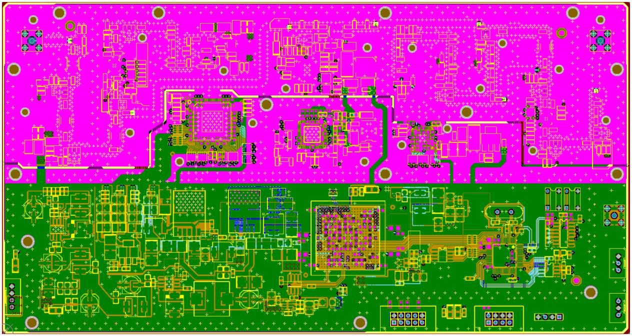
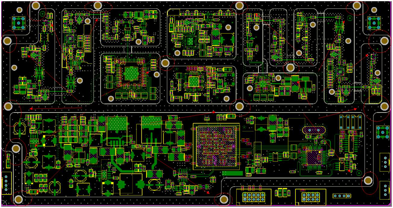
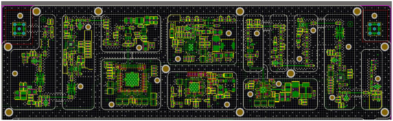
The mechanical structure of an RF product should be meticulously defined and reflected on the PCB board before the high frequency PCB layout process begins. This synchronization between Electrical Computer-Aided Design (ECAD) and Mechanical Computer-Aided Design (MCAD) ensures that the final assembly achieves the necessary electromagnetic shielding and structural robustness.
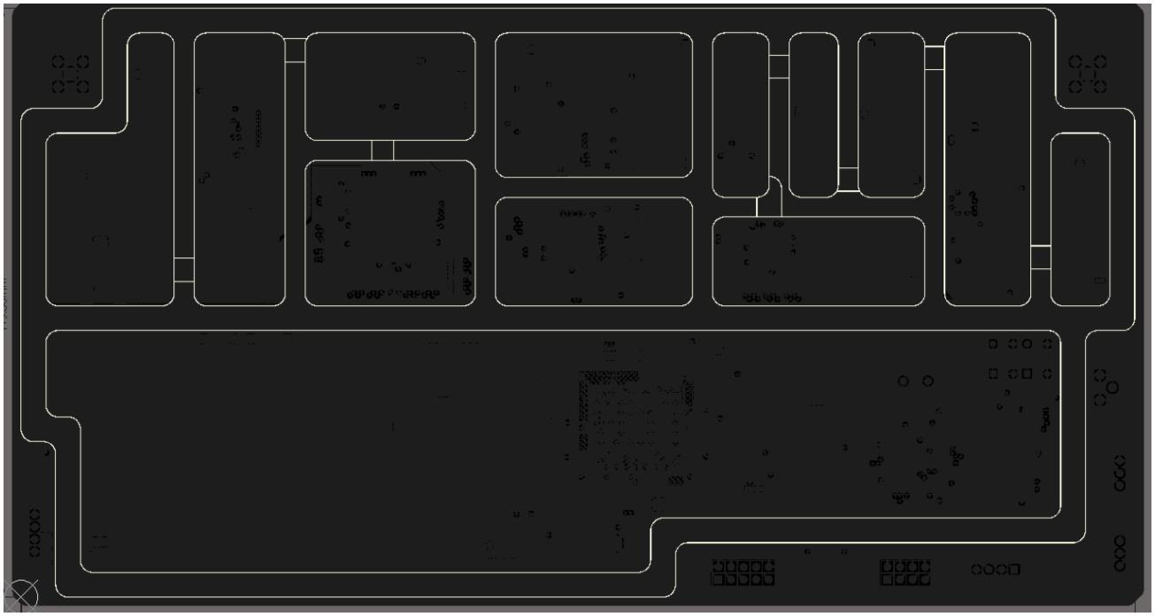
RF systems frequently utilize machined aluminum or copper-alloy housings that act as a Faraday cage to isolate sensitive circuits. Generally, the thickness of the outer side of the cavity shell is maintained at 4 mm to provide structural rigidity. The intermediate partition walls are typically 3 mm wide. These internal walls are crucial for dividing high-gain stages, such as the separation between a Low-Noise Amplifier (LNA) and a High-Power Amplifier (HPA), to prevent self-excitation through parasitic feedback loops.
Precision in these dimensions is vital; the compartment outlines on the PCB are recommended to be integer multiples of 0.5 mm, with a grid alignment of at least 0.1 mm, to allow structural manufacturers to achieve tighter error control.
To ensure stable electrical contact and optimal shielding, screw placement should follow specific functional logic. Screws are ideally placed at every intersection of the internal compartments. While sometimes difficult to achieve in dense layouts, screws should ideally be located at the four corners of the cavity shell. Critical components such as SMA heads or other RF connectors require mounting screws located in their immediate vicinity to prevent PCB deformation during cable insertion.
Section Summary: Seamless ECAD-MCAD synchronization and precise mechanical integration lay the structural foundation for effective electromagnetic shielding in RF products.
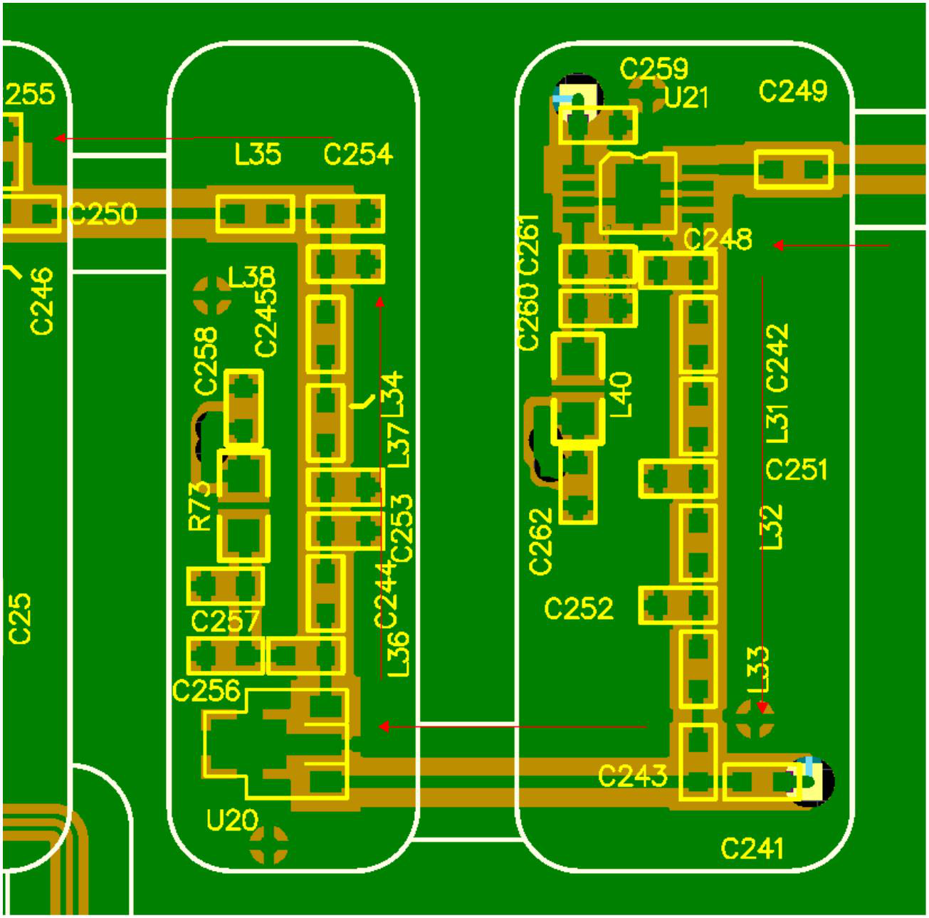
The layout of an RF system is driven by the signal flow, giving absolute priority to the radio frequency link over peripheral circuits.
An effective high frequency PCB layout should strictly follow the sequence of the schematic from input to output. The preferred layout geometry is a straight "One" shape or an "L" shape. These configurations offer the most direct paths and the highest degree of isolation between ports.
In scenarios where space constraints force the layout into a "U" shape, it is highly recommended to introduce a physical shielding compartment in the center of the "U" to isolate the input arm from the output arm. Without this isolation, electromagnetic coupling can cause the system to oscillate.
The layout of components around RF integrated circuits (ICs) typically adheres to manufacturer datasheets while optimizing for local signal flow. Passive components in a matching network should be grouped and placed as close as possible to the IC pins. This minimizes the physical length of the trace between the amplifier output and the matching network, effectively reducing the Standing Wave Ratio (SWR).
Section Summary: Prioritizing a direct, sequential signal flow minimizes parasitic variance and ensures system stability across the RF link.
> Recommend reading: 0201/0402 SMT Assembly: Tombstoning & Solder Defects
The choice of PCB material is the primary determinant of signal speed, loss, and thermal stability. Standard FR-4 becomes increasingly lossy above 1 GHz and is generally not recommended for high-performance RF designs.
High-performance RF laminates are engineered to provide a stable Dielectric Constant (Dk) and an ultra-low Dissipation Factor (Df).
| Property | Standard FR-4 | Rogers RO4350B | Taconic RF-35 |
|---|---|---|---|
| Dielectric Constant (Dk) | 4.2 – 4.8 (Unstable) | 3.48 ± 0.05 | 3.5 ± 0.05 |
| Loss Tangent (Df) | 0.018 – 0.025 | 0.0037 @ 10 GHz | 0.0018 @ 10 GHz |
| Thermal Conductivity | 0.25 W/m·K | 0.62 W/m·K | 0.45 W/m·K |
| Moisture Absorption | 0.15% | 0.05% | 0.02% |
As shown in the table, when comparing Rogers vs FR4, advanced RF laminates offer significantly lower loss tangent, higher thermal conductivity, and more stable dielectric properties, making them essential for high-frequency applications.
Because high-frequency materials carry a premium cost, engineers often utilize hybrid stackups. In a hybrid buildup, high-performance laminate is used for the critical signal layers, while cost-effective high-Tg FR-4 is used for internal layers carrying power and low-speed digital signals. When designing hybrid stackups, symmetry is paramount to prevent board warping during the high-temperature reflow process.
Section Summary: Selecting the appropriate substrate and utilizing symmetric hybrid stackups balances cost-efficiency with high-frequency performance reliability.
In the RF domain, PCB traces act as transmission lines guiding electromagnetic waves rather than simple point-to-point connections. Any deviation from a controlled 50 Ω characteristic impedance introduces reflections that degrade signal integrity — which is why impedance control PCB design is treated as a first-class constraint, not an afterthought, in the layouts described throughout this guide.
At the system level, two routing disciplines matter most: keeping traces as straight and short as possible from the schematic sequence described above, and avoiding sharp 90-degree corners in favor of 45-degree miters or arcs, which create impedance discontinuities. Surface finish also plays a role at high frequency — skin effect concentrates current on the conductor surface, which is why finishes such as Immersion Silver (IAg) or ENEPIG are commonly specified for mmWave boards.
> For the full impedance formula, trace geometry rules, and via stitching calculations: RF PCB Routing Design: Physical Layout to Manufacturing-Driven Impedance Control
Section Summary: Transmission line discipline — controlled impedance, smooth trace geometry, and frequency-appropriate surface finishes — underpins every layout decision in this guide.
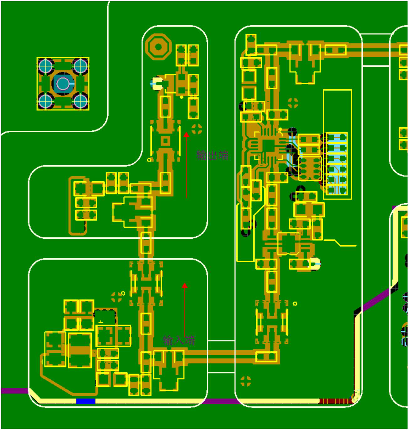
A solid RF grounding design strategy is the single most important factor in reducing electromagnetic interference (EMI) and maintaining consistent impedance.
RF designs employ multi-point grounding to ensure return currents have a low-inductance path. The primary ground plane should be located immediately beneath the signal routing layer. Discontinuities in the ground plane, such as slots or splits, should be strictly avoided under high-speed traces. A detour in the return current acts as an unintended antenna, creating massive EMI issues.
To maintain electrical continuity, arrays of stitching vias are placed throughout the ground copper. The distance between adjacent vias should generally not exceed one-tenth of the guided wavelength (λ/10) of the highest operating frequency.
| Frequency | Guided Wavelength (λ) | λ/10 Rule | λ/20 Rule |
|---|---|---|---|
| 868 MHz | 165.0 mm | 16.5 mm | 8.2 mm |
| 2.4 GHz | 62.5 mm | 6.2 mm | 3.1 mm |
| 5.8 GHz | 26.0 mm | 2.6 mm | 1.3 mm |
| 28 GHz | 5.3 mm | 0.5 mm | 0.2 mm |
This frequency-to-wavelength correlation dictates that higher frequencies demand exponentially denser via structures to suppress cavity resonances effectively. Via fences are highly recommended on both sides of grounded coplanar waveguides (GCPW) to enhance isolation.
Section Summary: A well-designed grounding strategy, featuring continuous reference planes and calculated via stitching, is essential for minimizing EMI and ensuring impedance stability.
High-frequency systems require a robust approach to both EMI mitigation and heat dissipation, particularly for power amplifiers based on GaN or LDMOS technologies.
In multi-cavity housings, grounding vias along the boundaries are typically punched in staggered rows. To further reduce contact resistance, a "window" is often opened in the solder mask where the board contacts the cavity walls, ensuring a low-impedance metal-to-metal connection.
Thermally, a dense array of thermal vias (e.g., 3 × 3 grid) is typically placed directly under high-power surface-mount components. Filling these vias with conductive epoxy or utilizing Metal Core PCBs (MCPCBs) ensures that excess heat does not shift the substrate's dielectric properties.
Section Summary: Integrating precision board-level shielding with robust thermal dissipation networks ensures consistent dielectric and signal performance under high power loads.
The leap to mmWave frequencies brings manufacturing tolerances to the forefront. At 10 GHz, a deviation of just 0.1 mm in trace width can alter impedance by 5 Ω, and via stubs as small as 1 mm can degrade signal integrity at 30 GHz. Translating a physics-correct design into a working board depends entirely on the fabricator's process control — HDI technology, back-drilling, and tight impedance tolerances are what stand between a simulated design and a working prototype.
> For material selection, process capability, and manufacturing DFM benchmarks in detail: RF PCB Manufacturing Guide: Material Selection, Process Control & Design Best Practices
Section Summary: Partnering with a fabricator that understands impedance tolerance and controlled-depth drilling is what turns a physics-driven layout into a reliable manufactured board.
| Turn Your RF PCB Design Into a Manufactured Board |
RF PCB manufacturing requires a factory that understands impedance tolerance, Rogers material handling, and controlled-depth drilling. NextPCB's multilayer stackup tool lets you configure your RF stackup and get a manufacturing-ready quote — with full DFM review included.
The electronics industry is undergoing a structural transformation characterized by the convergence of AI, high-density packaging, and sustainable manufacturing.
AI algorithms are becoming integral to the EDA workflow, automatically optimizing trace lengths for phase matching and predicting thermal hotspots. Meanwhile, Antenna-in-Package (AiP) technology is pushing frequencies beyond 100 GHz, integrating entire antenna arrays directly into the semiconductor package. This transition emphasizes the need for stable redistribution layers (RDL) and extreme thermal density management.
Machined cavity shielding provides higher isolation than a stamped shielding can because the compartment walls are integral to the housing and can be tuned to specific dimensions (e.g., 3 mm partition walls) that suppress resonance at the operating frequency. It's typically reserved for systems with high-gain stages, such as separating an LNA from an HPA, where a standard can's lower isolation isn't sufficient to prevent self-excitation.
As a general rule, stitching vias should be spaced no more than one-tenth of the guided wavelength (λ/10) at the highest operating frequency. At 2.4 GHz this is roughly 6.2 mm; at 5.8 GHz it tightens to about 2.6 mm. Denser λ/20 spacing is used where isolation requirements are stricter, such as along grounded coplanar waveguide (GCPW) edges.
Yes. Mechanical features like cavity walls, screw positions, and compartment outlines directly constrain where RF traces and components can be placed. Starting the electrical layout before the mechanical structure is defined typically forces rework later, since shielding compartments and screw clearances can't be added around a finished layout without disrupting the RF link.
RF power stages built on GaN or LDMOS generate concentrated heat that, if not managed, shifts the substrate's dielectric constant and detunes the circuit — not just a reliability risk but a signal integrity risk. This is why thermal vias are placed directly under power devices in dense arrays (e.g., a 3×3 grid) and often filled with conductive epoxy or built on a Metal Core PCB, rather than relying on general copper pour alone.
Compartment outlines are generally recommended to be integer multiples of 0.5 mm with a minimum grid alignment of 0.1 mm. Keeping to this grid gives the fabricator tighter, more predictable error control when machining or routing the cavity walls against the PCB outline.
Successful RF PCB design in the high-GHz and mmWave eras requires a fundamental shift from a "connectivity" mindset to a "wave propagation" mindset. Signal integrity is a byproduct of meticulous physical layout, rigid adherence to return path discipline, and the strategic use of advanced low-loss substrates. By integrating structural shielding and manufacturing constraints early in the physics-driven design phase, engineers can consistently deliver hardware that meets the stringent link budget and EMI requirements of next-generation wireless communications.

Still, need help? Contact Us: support@nextpcb.com
Need a PCB or PCBA quote? Quote now

