NextPCB Capabilities
 PCB Assembly
 Layer Buildup
 SMD-Stencils
 PCB Design-Aid & Layout
 Mechanics
 Quality
 Drills & Throughplating
 Factory & Certificate





Blistering is one of the most damaging failure modes an HDI multilayer board can develop during lead-free reflow — severe enough, in some cases, to halt a production line outright. Unlike the Rogers/FR4 via-hole delamination covered in our earlier analysis, HDI blistering is a separation between the second-lamination PP sheet and the browned copper surface of the next layer (L2), and it follows a fairly well-understood "volatiles → expansion pressure → interfacial bond strength" physical model. This article walks through the characteristics of blistering, the mechanism behind it, and the main levers for suppressing it, for PCB process and quality engineers.
1. The Blistering Phenomenon
1.1 Description and Distribution Pattern
During lead-free reflow, separation between the second-lamination PP sheet and the browned copper surface of the next layer (L2) in an HDI board's build-up is what's referred to as blistering. Under cross-section inspection, blistering is often severe — in some cases traces are torn apart outright, making the risk far from cosmetic. Cross-section analysis across multiple cases points to three consistent distribution patterns:
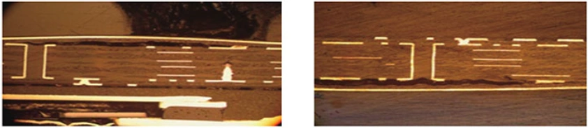
Photo placeholder — replace with your own fab/lab imagery. Referenced case photo source: An Wei & Zeng Fulin, Fundamentals of PCB Technology for Communication Products and Their Applications (2021).
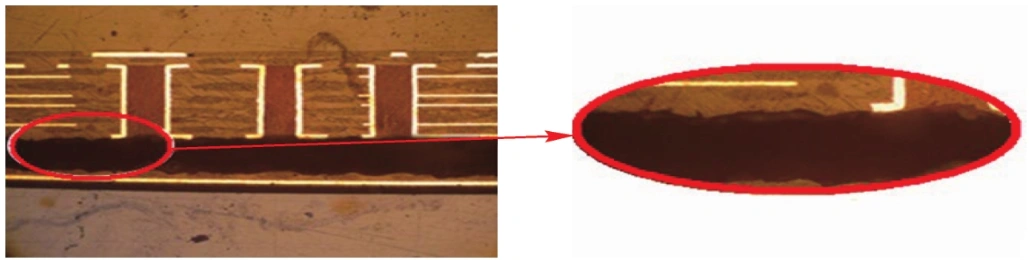
Photo placeholder — replace with your own fab/lab imagery. Referenced case photo source: An Wei & Zeng Fulin, Fundamentals of PCB Technology for Communication Products and Their Applications (2021).
- Distribution across the board surface: blistering almost always occurs under large copper foil areas with no hole openings (micro-vias) — in other words, large, unbroken copper coverage without any opening is the highest-risk zone.
- Distribution through board thickness: blister locations concentrate between the outer layer and the next layer in, and mostly sit directly beneath large copper areas and directly above buried vias.
- Location relative to via density: blister sites cluster in regions with dense L1–L2 buried vias, which points to buried vias as a real contributing factor rather than a coincidence.
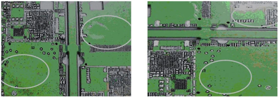
Photo placeholder — replace with your own fab/lab imagery. Referenced case photo source: An Wei & Zeng Fulin, Fundamentals of PCB Technology for Communication Products and Their Applications (2021).
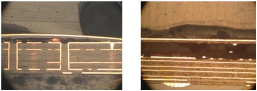
Photo placeholder — replace with your own fab/lab imagery. Referenced case photo source: An Wei & Zeng Fulin, Fundamentals of PCB Technology for Communication Products and Their Applications (2021).
2. The Physical Mechanism Behind Blistering
Breaking blistering down into a continuous physical process makes it easier to see how the problem builds up step by step before it finally shows up as a visible defect:
- Normal state: at moderate ambient temperature, bonding between L1 and L2 in an HDI multilayer board is sound, with nothing unusual.
- Heat-driven outgassing: as the reflow ramp progresses, volatiles absorbed at buried vias and inner layers — including moisture — are steadily released and expand under heat.
- Gas accumulation: the released gas collects at the interface between the buried via opening and the PP bonding sheet.
- Expansion pressure build-up: as temperature keeps rising, more gas accumulates near the via opening, generating substantial expansion pressure that pushes to separate the L2 browned surface from the PP sheet.
- Separation / blistering: once the expansion pressure (f) exceeds the adhesion force (F) between the browned surface and the PP sheet, that pressure forces the two apart and blistering occurs.
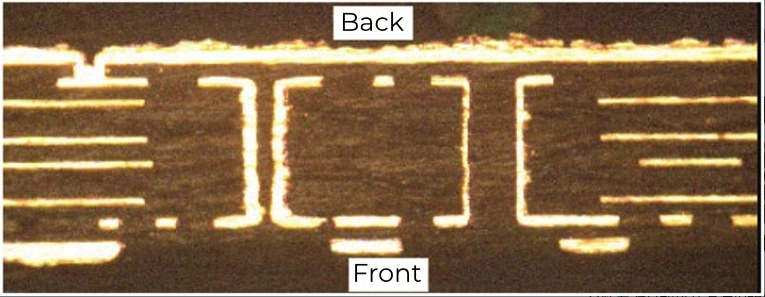
Photo placeholder — replace with your own fab/lab imagery. Referenced case photo source: An Wei & Zeng Fulin, Fundamentals of PCB Technology for Communication Products and Their Applications (2021).
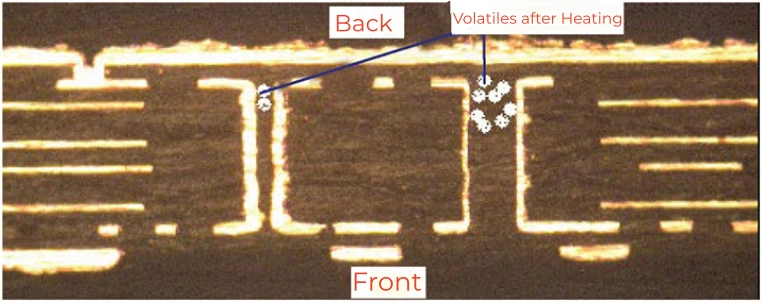
Photo placeholder — replace with your own fab/lab imagery. Referenced case photo source: An Wei & Zeng Fulin, Fundamentals of PCB Technology for Communication Products and Their Applications (2021).
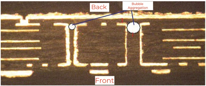
Photo placeholder — replace with your own fab/lab imagery. Referenced case photo source: An Wei & Zeng Fulin, Fundamentals of PCB Technology for Communication Products and Their Applications (2021).
The most important variable in this whole model is really the balance between expansion pressure (f) and adhesion force (F) — and that balance is exactly what determines which form the blister takes:
- Point blistering: when the final expansion pressure (f) stays below the adhesion force (F) between the browned surface and PP sheet (f < F), only a small bubble is left at the inner-layer via opening — visible as a small localized bump on the board surface.
- Block blistering: when the final expansion pressure (f) exceeds the adhesion force (F) (f > F), a large-area separation occurs along the L2 browned surface/PP sheet interface, producing an obvious block-shaped delamination that is considerably more damaging than a point blister.
It's worth noting that when a PCB heats up, some of the free-volume water can escape through microscopic pore paths in the base material, which reduces the molar volume fraction of water that could otherwise collect at voids or micro-cracks — a natural outgassing mechanism that actually helps limit blistering. But if the PCB surface is covered by a large area of copper foil, this flips: the large copper area above a buried via blocks the escape path for water vapor trying to vent outward under heat, raising the vapor pressure trapped in micro-cracks and substantially increasing blistering risk. This is exactly why blistering shows up almost exclusively under "large, unbroken copper areas."
>> Worried about copper coverage over buried vias in your HDI stack-up? NextPCB's free HQDFM analysis tool flags large unbroken copper areas above buried vias — the exact risk pattern described above — before your design goes to fab.
3. Three Key Factors Behind Blistering
3.1 Necessary Condition: A Source of Volatiles (PCB Moisture Absorption)
The root source of a PCB's volatiles is moisture absorbed during manufacturing. PCB constituent materials — fiberglass weave and resin — have a strong affinity for water and absorb moisture readily. Water in a PCB mostly resides within resin molecules and at macroscopic physical defects such as voids and micro-cracks. The absorption rate and equilibrium moisture content of epoxy resin are largely governed by free volume and the concentration of polar groups: larger free volume means a faster initial absorption rate, and polar groups' affinity for water is the main reason epoxy resin has relatively high moisture uptake capacity to begin with.
As PCB temperature rises during lead-free reflow, water bound in free volume and hydrogen-bonded to polar groups gains enough energy to diffuse through the resin, migrating outward and accumulating at voids or micro-cracks — raising the molar volume fraction of water at those sites. At the same time, the saturated vapor pressure of water climbs as soldering temperature increases.
The scale of this effect is worth spelling out with real numbers: at 224°C, the saturated vapor pressure of water is about 2500 kPa; at 250°C, it climbs to roughly 4000 kPa; and by 260°C it can reach around 5000 kPa. Once the bond strength between material layers drops below the saturated vapor pressure the trapped water can generate, blistering occurs. Pre-solder moisture absorption is therefore one of the leading causes of PCB delamination and blistering.
| Temperature (°C) | 180 | 198 | 212 | 224 | 234 | 243 | 250 | 260 | 285 |
|---|---|---|---|---|---|---|---|---|---|
| Saturated Vapor Pressure (kPa) | 1000 | 1500 | 2000 | 2500 | 3000 | 3500 | 4000 | 5000 | 7000 |
Moisture picked up during storage and assembly of finished PCBs matters just as much. HDI multilayer boards are moisture-sensitive components, and PP sheets in particular absorb moisture readily — the absorption rate rises with both storage time and relative humidity. Comparing three humidity levels (30%, 50%, and 90% RH), higher relative humidity produces a higher equilibrium moisture content, and most of the uptake happens quickly early in storage before leveling off.
The gap between vacuum and non-vacuum packaging tells a similar story: non-vacuum-packaged material typically absorbs about 1.5 to 2 times as much moisture as vacuum-packaged material, and while that gap narrows somewhat as standing time increases, vacuum packaging consistently keeps moisture absorption lower.
| Standing Time | Non-Vacuum Absorption (%) | Vacuum Absorption (%) | Non-Vacuum / Vacuum Ratio |
|---|---|---|---|
| 1 week | 0.08823 | 0.04549 | 1.94 |
| 2 weeks | 0.09716 | 0.06240 | 1.56 |
| 3 weeks | 0.11663 | 0.07857 | 1.48 |
| Packaging | Storage Time | Pre-Bake Weight (g) | Post-Bake Weight (g) | Moisture Content (g) | Moisture Rate (%) |
|---|---|---|---|---|---|
| Vacuum | 1 week | 53.6329 | 53.6085 | 0.0244 | 0.04549 |
| 2 weeks | 53.0448 | 53.0117 | 0.0331 | 0.06240 | |
| 3 weeks | 53.20 | 53.1582 | 0.0418 | 0.07857 | |
| Non-Vacuum | 1 week | 52.9292 | 52.8825 | 0.0467 | 0.08823 |
| 2 weeks | 53.0037 | 52.9522 | 0.0515 | 0.09716 | |
| 3 weeks | 54.5318 | 54.4682 | 0.0636 | 0.11663 |
Panels pulled from inventory after two months in original packaging (FR4/OSP, vacuum-sealed) showed noticeably elevated moisture content — already at a level associated with blistering risk, as shown in the storage-period sampling below.
| Sample | Pre-Bake Weight (g) | Post-Bake Weight (g) | Moisture Rate (%) |
|---|---|---|---|
| Sample 1 | 31.1966 | 31.1478 | 0.1564 |
| Sample 2 | 31.1825 | 31.1313 | 0.1642 |
| Sample 3 | 31.8031 | 31.7516 | 0.1619 |
| Sample 4 | 31.5299 | 31.4784 | 0.1633 |
| Sample 5 | 31.2184 | 31.1658 | 0.1685 |
Under normal storage conditions, moisture content climbs steadily as time passes. Once a board is more than two months past its manufacture date, elevated moisture uptake meaningfully raises blistering risk — which is also why the same reflow batch can sometimes show a clean first run of boards followed by blistering later in the same lot, if the later boards sat in storage longer.
3.2 Sufficient Condition: Poor Adhesion Between PP Sheet and Copper Foil
Cross-section analysis consistently shows blister sites sitting exactly at the second-lamination PP sheet/copper foil (browned surface) interface, which makes this interface the sufficient condition that determines whether blistering actually happens.
Copper in its metallic state is a polar substance, and many adhesives naturally bond poorly to it. Untreated copper foil, even paired with a high-performance adhesive, can't achieve adequate adhesion or heat resistance — which is exactly the problem browning treatment exists to solve. The browning process itself has gone through several generations of improvement:
- Early treatment chemically formed a reddish-brown cuprous oxide (Cu₂O) layer on the copper surface. Adhesion at room temperature was acceptable, but the layer tended to delaminate around 200°C due to the thermal instability of Cu₂O.
- In the 1960s, researchers at Toshiba in Japan found that a specialized chemical treatment produced a fine-grained, black velvet-like cupric oxide (CuO) film that bonded firmly to the copper surface with substantially better thermal stability — this became the widely adopted "black oxide" process.
- By the mid-1990s, European and American manufacturers had moved to a newer chemical-oxidation browning process for inner-layer imaging on multilayer boards, which has since replaced the older black oxide process across the industry.
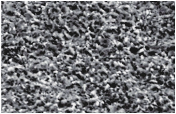
Photo placeholder — replace with your own fab/lab imagery. Referenced case photo source: An Wei & Zeng Fulin, Fundamentals of PCB Technology for Communication Products and Their Applications (2021).
The core mechanism of modern browning chemistry is a controlled oxidation reaction in the browning tank (copper reacting with sulfuric acid, hydrogen peroxide, and the tank's proprietary browning formula) that roughens the base copper surface at the microscopic level. The micro-etching effect of the hydrogen peroxide produces a bonding surface area roughly six to seven times that of an untreated, smooth copper surface, while simultaneously depositing a thin organometallic film chemically bonded to the base copper. Once adhesive fills in the roughened topography, mechanical interlocking adds further bond strength on top of the chemical bond.
But browning performance isn't simply "thicker film, stronger bond." In practice, the factors that actually determine adhesion quality are more granular:
- Browning chemistry selection: different browning formulations show very different resistance to repeated reflow. Under identical conditions (high-Tg material, 10-second reflow dwell), one formulation withstood 12 lead-free reflow passes without blistering, while a comparison formulation began blistering around the 9th pass — making chemistry selection a primary lever on the ceiling of achievable bond strength.
| Browning Chemistry | 1 | 2 | 3 | 4 | 5 | 6 | 7 | 8 | 9 | 10 | 11 | 12 |
|---|---|---|---|---|---|---|---|---|---|---|---|---|
| Formulation A | 0 | 0 | 0 | 0 | 0 | 0 | 0 | 0 | 0 | 0 | 0 | 0 |
| Formulation B | 0 | 0 | 0 | 0 | 0 | 0 | 0 | 0 | 1 | 3 | — | — |
- Bath composition monitoring during production: browning bath concentration and active-ingredient levels decay with use and need continuous monitoring and replenishment.
- Browning film thickness control: bond strength, acid/alkali resistance, corona resistance, and heat resistance are all tied to film structure and thickness — but thicker isn't automatically better, and film thickness needs to be controlled within a defined process window.
- Browning layer contamination: in one real blistering case, peeling back the failed area revealed visible contamination of the browning layer — the resin had fully separated from the contaminated browning surface, which showed clear signs of contamination. The contaminated section never achieved proper adhesion to the PP sheet during lamination, and the board later developed blistering during SMT assembly. Investigation traced the root cause to a process error: high-Tg material had mistakenly been run through the lamination and curing schedule for ordinary material — a reminder that process discipline and material segregation matter just as much as the browning chemistry itself.
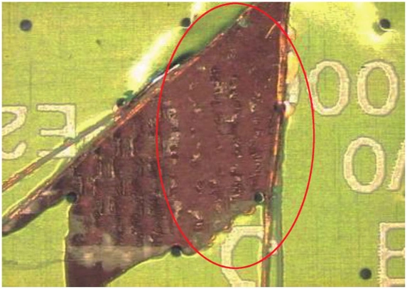
Photo placeholder — replace with your own fab/lab imagery. Referenced case photo source: An Wei & Zeng Fulin, Fundamentals of PCB Technology for Communication Products and Their Applications (2021).
3.3 Trigger Factor: Unsuitable Reflow Temperature Selection
Both the necessary and sufficient conditions for blistering ultimately need temperature to trigger a visible failure. The volume of volatiles in a multilayer board and their expansion pressure both increase with reflow temperature, while the adhesion between the browning layer and PP sheet decreases as temperature rises — meaning higher temperature pushes the system toward blistering from both directions at once. That's why optimizing the reflow temperature profile around a specific product's characteristics is such an effective lever for suppressing blistering.
Industry consensus on this point is fairly well established. U.S. microelectronics packaging expert C.G. Woychik has noted that when using conventional SnPb alloy for reflow, components and PCBs can tolerate a maximum temperature of 240°C, whereas JEDEC standards set the maximum at 260°C for SnAgCu (lead-free) alloy. That higher ceiling can compromise the integrity of electronic assemblies — particularly multilayer-structure materials, which are prone to interlayer separation, especially newer materials carrying more moisture. Combined with elevated internal moisture, higher temperature can drive widespread delamination across commonly used build-up structures such as HDI multilayer PCBs.
U.S. electronics assembly and soldering expert J.S. Hwang has made a similar point: given that lead-free material melting points run higher than the SnPb eutectic melting point (183°C), keeping reflow temperature as low as practical calls for a well-designed reflow profile. Given current production constraints — existing SMT infrastructure and the thermal characteristics of both components and PCBs — lead-free reflow peak temperature should be held around 235°C.
Putting this together, for lead-free reflow on HDI multilayer PCBs using SnAgCu solder alloy, a peak temperature of 235–240°C (not exceeding 245°C) is the recommended range. Large-scale production validation backs this up: as long as adequate wetting temperature is still achieved, keeping peak reflow temperature within this range has a clear effect on suppressing blistering — the higher the temperature climbs beyond it, the greater the blistering risk.
3.4 Contributing Factor: Poor Volatile Escape Paths
Cross-section analysis shows blister sites almost always occur under large areas of copper foil directly above buried vias. This design pattern creates manufacturability problems on three fronts: it restricts the escape path for volatiles (including moisture) trapped at buried vias and interlayer interfaces during heating; it worsens temperature-distribution uniformity across the board during reflow; and it interferes with dissipating thermal stress during soldering, concentrating stress and worsening interlayer separation in HDI multilayer PCBs. In short, poor copper-pour design on HDI multilayer products actively contributes to blistering in lead-free processing.
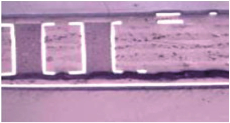
Photo placeholder — replace with your own fab/lab imagery. Referenced case photo source: An Wei & Zeng Fulin, Fundamentals of PCB Technology for Communication Products and Their Applications (2021).
4. Solutions for Blistering
Working from the necessary condition — sufficient condition — trigger factor — contributing factor framework above, suppressing blistering calls for action on four fronts at once:
4.1 Eliminate the Necessary Condition: Prevent PCB Moisture Absorption
- Tighten temperature and humidity control at key process steps: every stage of PCB production — raw material storage, PP sheet slitting, layer stack-up storage, browning through final packaging — needs strict temperature and humidity control. Finished multilayer PCBs are moisture-sensitive components just like MSD-rated components, and should be managed to MSD-level moisture protection standards (temperature ≤30°C; humidity ≤60% RH).
- Add a baking step at critical process points: many PCB manufacturers, for various reasons, can't move material through process steps promptly, leading to backlogs of raw material, semi-finished, or finished product. Adding a baking step at a critical point — for example, after browning but before lamination — effectively removes moisture content before it becomes a problem; boards should move to lamination promptly after drying rather than sitting exposed.
- Address storage moisture uptake: on one side, adopt JIT (Just In Time) production so boards go into use quickly after leaving the factory; on the other, improve packaging — vacuum-sealed packaging paired with a denser high-barrier aluminum-foil vacuum layer, plus desiccant and a humidity indicator card inside the package. For boards whose moisture content has already climbed, baking under controlled conditions (based on the specific laminate and surface finish) can remove moisture — a bake temperature of ≤125°C for 4 hours is a reasonable starting point.
4.2 Strengthen the Sufficient Condition: Increase Interlayer Bond Strength
- Use a high-quality browning chemistry to raise PCB interlayer bond strength.
- Tightly control the interval between browning and lamination to limit moisture pickup in that window.
- Add a bake step after browning to effectively remove resin volatiles and residual moisture.
- Strengthen incoming material quality control so the final laminate consistently exhibits low moisture absorption, good interlayer adhesion, and dimensional stability.
4.3 Optimize the Reflow Temperature Profile
Large-scale production validation shows that, in lead-free reflow, keeping the peak reflow temperature on the lower side — around 235°C, not exceeding 245°C — while still achieving adequate wetting temperature has a clear effect on suppressing blistering. Higher temperature translates directly into higher blistering risk.
4.4 Avoid Large, Unbroken Copper Pour Designs
A large copper area directly above a buried via blocks the escape path for water vapor trying to vent outward under heat, raising blistering probability. Wherever it doesn't compromise design performance, avoiding large unbroken copper pours — or adding openings in large copper areas to give trapped water vapor somewhere to vent — measurably improves blistering outcomes.
>> These findings inform how NextPCB manages moisture control and browning process discipline for HDI builds internally — from incoming material handling to bake schedules and reflow profile tuning. See our HDI & high-density manufacturing capabilities for the process controls we apply by default.
5. Summary
HDI blistering is fundamentally a race between "how fast volatiles can escape" and "how strong the interlayer bond is." Wherever volatiles can't vent quickly enough and bond strength can't keep pace with rising expansion pressure, blistering happens — the only question is whether it shows up as a point blister or a block. Moisture control across the PCB supply chain, browning process discipline, reflow temperature profile optimization, and avoiding large copper coverage over buried vias in the design itself are all necessary levers, and none of them substitutes for the others.
>> Working on an HDI stack-up with dense buried vias?
Send us your layer stack and copper-pour layout — our engineering team will flag blistering risk factors like the ones above before you commit to fabrication.
FAQ
What causes blistering in HDI PCBs during lead-free reflow?
Blistering happens when trapped moisture and other volatiles inside the board vaporize during reflow, building up expansion pressure between the browned copper surface and the PP bonding sheet near buried vias. When that expansion pressure exceeds the bond strength at the interface, the layers separate, producing either a small point blister or a larger block-type delamination depending on how far the pressure exceeds the bond strength.
Why does blistering concentrate under large copper areas above buried vias?
A large, unbroken copper foil area above a buried via blocks the natural path for water vapor to escape through the board during heating. Without an escape route, vapor pressure builds up faster in that pocket than it would in an area with hole openings or smaller copper coverage, making blistering far more likely directly beneath large copper regions.
What reflow peak temperature is recommended to reduce blistering risk on HDI boards?
For SnAgCu lead-free solder, industry practice and large-scale production validation generally point to a peak reflow temperature of 235 to 240 degrees Celsius, not exceeding 245 degrees Celsius, as long as adequate wetting temperature is still achieved. Lower peak temperatures reduce both the expansion pressure of trapped volatiles and the thermal stress on the browned bond interface.
Reference
The referenced case photography in this article are drawn from: An Wei, Zeng Fulin (eds.), Fundamentals of PCB Technology for Communication Products and Their Applications, People's Posts and Telecommunications Press, 2021.