Support Team
Feedback:
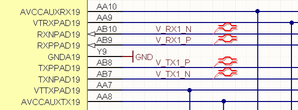
support@nextpcb.comIn the menu Place>>Directive places differential pair instructions for the differential network. The differential pair network name must be followed by "_N" and "_P". After placing the instruction on the differential network, its parameters must be configured, including the DifferentialPair name and the True parameter.
When designing synchronization, the differential pair will be converted from the schematic to the pcb.

"Place directives on the schematic to define differential pairs."
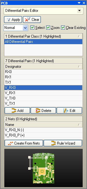
Viewing and Managing Differential Pairs in the PCB You can view and manage defined differential pairs by selecting “Differential Pairs Editor” from the drop-down list in the PCB panel.

"Differential pairs can be viewed and managed in the Differential Pair Editor."
Defining a differential pair in the PCB not only defines the differential pair in the schematic, but also defines the differential pair in the PCB editor.
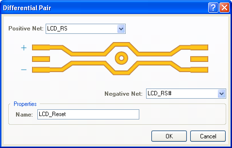
Select the Differential Pairs Editor mode in the PCB panel and click the Add button. In the Differential Pair dialog that pops up, select the positive and negative networks in the existing network, name the differential pair, and click OK.

"Quickly create pairs from the named nets."
The definition of the differential pair can also be made by the network name. For a differential pair, the names have the same prefix and are distinguished by different post-ends, such as TX0_P or TX0_N. Click the Create From Nets button in the PCB panel to open the Create Differential Pairs From Nets dialog. Use filters at the top of the dialog to filter out differential pairs from existing networks.
Applicable design rules for routing differential pairs must be configured in the three design rules in the PCB Rules and Constraints Editor dialogs (called in Design>>Rules):
Routing Width - Defines the width of the differential pair line, which can be the actual physical width or automatically calculated from the user-defined characteristic impedance. Set the scope of the rule to the target device of the differential pair, such as *InDifferentialPair*.
Differential Pairs Routing - Defines the spacing and decoupling length of the differential network lines (paired traces lose coupling when the interval width is greater than the Max Gap setting). Set the scope of the rule to the target device of the differential pair, such as *IsDifferentialPair*.
Electrical Clearance - Defines the spacing of individual devices including the same network and different networks (between pads and pads, between pads and lines). Set the scope of the rule to the target device of the differential pair, such as *InDifferentialPair*.
The length of the differential pair line can be adjusted via the Interactive Diff Pair Length Tuning (in the Tools menu) function. This feature allows real-time adjustment of the desired length and tolerance of the differential pair line and has different options to adjust the network line length by adding various undulating corrugated lines.
The jurisdiction of the design rules that set the design rules defines the scope of the rules. The differential pair can define the jurisdiction of the design rule by the following search condition example.
InDifferentialPairClass('All Differential Pairs') - All paired networks belong to the differential pair class "All Differential Pairs"
InDifferentialPair('D_V_TX1') -* defines two networks in the differential pair name "D_V_TX1"
(IsDifferentialPair And (Name = 'D_V_TX1')) - Define the differential pair with the network name "D_V_TX1"
(IsDifferentialPair And (Name Like 'D')) -* Defines a differential pair with all network names starting with the letter "D". Using the differential pair wizard to define the rule. Click on the Rule Wizard button in the PCB face differential pair editor. Design rules are set. Note that the scope of the rule created here is the object selected before clicking the Rule Wizard button. If a pair of differential pairs is selected, the jurisdiction of the design rule is a pair of differential pairs, if the class of a differential pair is selected The domain of the design rule is the class of the differential pair.
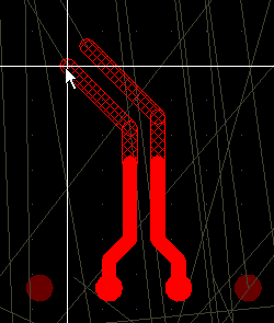
The differential pair wiring differential pair wiring is performed in one pair, that is, the two networks are simultaneously wired. To route differential pairs, select Differential Pair Routing from the menu or use the right mouse button menu to bring up the differential pair routing tool. At this point, the user will be prompted to select the wiring object, and click on any network of the differential pair to start wiring. The figure below shows the differential pair wiring.
In the differential pair wiring, the interactive wiring mode that encounters the first obstacle to stop or ignore the obstacle is used, and the SHIFT+R shortcut key is used for cyclic switching. Differential pair routing and interactive routing have some of the same shortcuts. Use the * key in the numeric keypad to change layers. Press the 5 shortcut to cycle through the possible via modes. Press the Shift+F1 shortcut to display all possible shortcuts.

"Differential pairs are routed simultaneous."
Applying a Differential Pair Indicator By adding a differential pair indicator to the border of the coverage indicator, you can quickly create differential pairs based on a differential network within the coverage area.
Quickly create differential pairs based on differential networks captured in the coverage area
The comprehensive differential pair in the FPGA design, including pin swapping, supports modern FPGAs, providing a large number of pins for user-configured differential pairs even in some inexpensive products. In order to facilitate the design work, Altium Designer fully supports FPGA-based differential pairing in FPGA and PCB design.
In FPGA design, a single network can be defined on differential I/O, such as the LVDS standard, so that the software maps a pair of physical networks into the PCB design. This process can be controlled by the FPGA Signal Manager. The design compiler can also determine if the pins are used as differential pairs in the PCB design and correctly mapped into the FPGA device.
Support for Signal Integrity in Differential Pairs Altium Designer's signal integrity analysis provides comprehensive support for differential pair simulation. Using the LVDS standard in the FPGA pins ensures that the correct signal integrity model is used.
Still, need help? Contact Us: support@nextpcb.com
Need a PCB or PCBA quote? Quote now