

 Printed Circuit Boards
 Surface
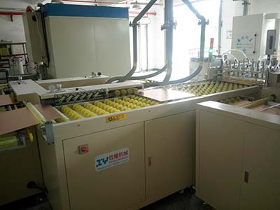
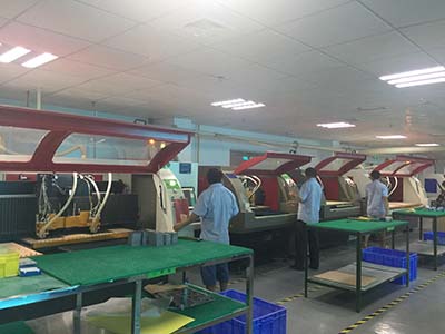
 PCB Assembly
 Layer Buildup
 Online Tools
 PCB Design-Aid & Layout
 Mechanics
 SMD-Stencils
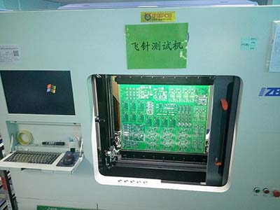
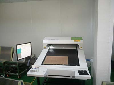
 Quality
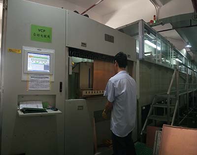
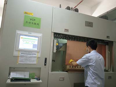
 Drills & Throughplating
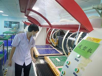
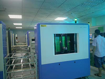
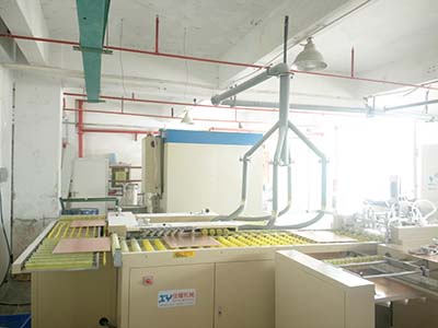
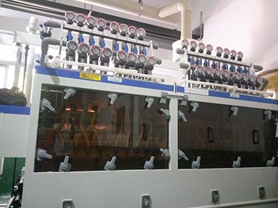
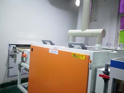
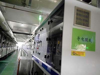
 Factory & Certificate


-
-
-
Characteristic Impedance PCB Design of Material Composition Structure
Design of the material composition of the board
3590 3 0 Shares
-
-
-
-
-
-
-
"Smart layout" PCB board
5 Tips
459 1 0 Shares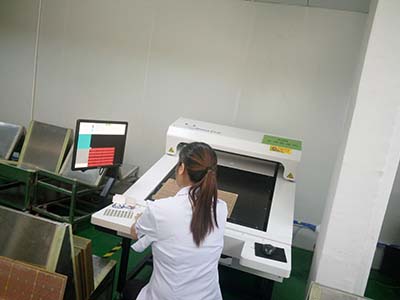
-
-
-
PCB layout technology
In general, the most basic process of designing a board can be divided into three major steps.
3894 1 0 Shares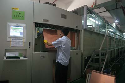
-
-
How to avoid transmission line effects in high speed PCB design?
4 methods and solutions
3782 1 0 Shares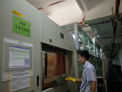
-
-
-
-
-
Categories
Recommended Article:
- Selecting an ISO 13485 PCB Assembly Partner for Medical Devices
- How to Select an Advanced Automotive-Grade PCB Manufacturer
- OpenClaw Neural-Hardware Accelerator Program
- Rescuing HDI Yield: Pulse Plating & Pre-treatment for Microvia Reliability
- PCB Design for IoT Devices: Layout, Stackup, Power & Reliability Challenges
- 10 HDI PCB Manufacturers Delivering High‑Density Interconnect Solutions
- Back-drill vs Blind/Buried Vias: Cost, Signal Integrity, and Manufacturing Scalability
- At What Frequency Node Must We Switch from FR-4 to Rogers?
- Ultimate PCB Assembly Guide: Prototyping to Mass Production | NextPCB
- How to Reduce PCB Assembly Costs Without Sacrificing Quality (2026 DFM Guide)