Table of Contents
- 1. Introduction: When Clock Meets Wavelength
- 2. The Deep Reality: Time Domain vs. Frequency Domain
- 3. The Art of Materials: Balancing Dk and Df
- 4. Routing: Two Different Playbooks
- 5. Manufacturing and Testing Hurdles
- 6. Real-World Pitfalls: Lessons from the Lab
Key Insights:
- Mastering the Fundamentals: Clearly distinguish between High-Speed Design (focusing on signal transition speed and clock alignment) and High-Frequency Design (focusing on wavelength and energy loss).
- Material Selection Logic: A look at the trade-off between cost and Dissipation Factor (Df) for high-speed boards versus the strict requirement for Dielectric Constant (Dk) stability in high-frequency boards.
- Design Strategy Comparison: A breakdown of "Length Matching & Timing" tactics for high-speed routing versus the "Shortest Path & Impedance Matching" rules for high-frequency routing.
- Practical Pro Tips: Real-world solutions including Hybrid Stackups for cost reduction, specialized via handling, reverse-treated foil (RTF), and validation methods like Eye Diagrams and S-parameters.
1. Introduction: When Clock Meets Wavelength
In the early stages of PCB design, many engineers fall into a common trap: assuming that if a board has a high frequency, it’s a "High-Frequency" board, and if it runs fast, it’s a "High-Speed" board. While they sound similar, choosing the wrong design path based on this intuition can lead to costly failures.
In essence, High-Speed PCB design is a race against time. It focuses on the time-domain performance of digital signals—ensuring that billions of 0s and 1s flip precisely at the right nanosecond without getting garbled. We focus on rise/fall times, setup times, and hold times.
In contrast, High-Frequency PCB design is a battle against energy loss. It focuses on the frequency-domain purity of analog or RF signals—ensuring that weak signals travel through the board with minimal attenuation or interference. Here, wavelength, power, and phase are the stars of the show.
Understanding this fundamental split is the first step toward making the right calls in material selection and routing strategy.
2. The Deep Reality: Time Domain vs. Frequency Domain
2.1 High-Speed PCB: It’s All About the "Edge"
When talking about high-speed circuits, the clock frequency (MHz or GHz) can be a misleading metric. What truly defines a circuit as "high-speed" is the Rise Time (Tr) of the signal.
Imagine a 50MHz clock signal with a very sharp 1ns rise time. According to Fourier analysis, this signal contains extremely rich high-frequency harmonic components. If the PCB isn't designed to handle these harmonics, the edges will round off, turning a clean square wave into something resembling a sine wave, eventually leading to data errors.
In high-speed designs (like DDR5 or PCIe 6.0), engineers spend most of their energy on Signal Integrity (SI). This means tackling reflections caused by impedance diconnects, crosstalk between traces, and ground bounce from messy reference planes.
2.2 High-Frequency PCB: Keeping the "Wave" Intact
For high-frequency circuits (typically RF/Microwave circuits above 1GHz), the signal is no longer just a voltage level; it’s an electromagnetic wave propagating along a transmission line.
At these frequencies, Skin Effect and Dielectric Loss become the primary enemies. Current no longer flows through the whole conductor but crowds onto a thin layer at the surface. Meanwhile, the PCB material itself "soaks up" some of the signal's energy and turns it into heat.
The goal here is fidelity. Whether it’s a 5G base station or an automotive millimeter-wave radar, the designer is fighting to maintain power levels and phase characteristics while avoiding Passive Intermodulation (PIM).
2.3 Quick Comparison Table
| Feature |
High-Speed PCB |
High-Frequency PCB |
| Signal Type |
Digital Square Wave (Timing) |
Analog Sine/Modulated Wave (Energy) |
| Key Challenge |
Reflections, Crosstalk, Jitter |
Insertion Loss, Phase Noise, VSWR |
| Impedance |
Focus on Differential pair & Common-mode |
Focus on absolute 50Ω/75Ω accuracy |
| Routing Mantra |
Match lengths, Use serpentine traces |
Keep it short, Keep it simple, Avoid vias |
| Sensitivity |
Sensitive to Via-induced discontinuities |
Sensitive to Copper roughness & Corner effects |
3. The Art of Materials: Balancing Dk and Df
The substrate determines the performance ceiling of your product. There are two "magic numbers" you need to know: the Dielectric Constant (Dk) and the Dissipation Factor (Df).
High-Speed Materials: Hunting for Value
>> See Deatailed High-Speed Material List
For high-speed digital circuits, the priority is preventing the medium from "filtering out" the signal's harmonics. The lower the Df value, the less the signal rounds off.
However, high-speed boards are often large and multi-layered (like server motherboards), making them very cost-sensitive. Engineers usually skip expensive PTFE and opt for Enhanced FR-4 or Low-loss Resins (e.g., Panasonic Megtron series or Isola Tachyon). These offer a great Df (between 0.002 and 0.005) while remaining easy to manufacture.
High-Frequency Materials: Stability is King
>> Material Selection for High-Frequency PCBs
In RF design, Dk stability is everything. A tiny shift in Dk changes the impedance of your line, causing reflections or shifting the center frequency of a filter.
This is why high-frequency boards often use PTFE (Teflon) or Ceramic-filled Hydrocarbons (like Rogers RO4000 series).
- PTFE offers the lowest Dk (∼2.1) and near-zero loss, ideal for radar, but it’s "squishy" and hard to process.
- Rogers 4000 is the industry workhorse. It processes like FR-4 but performs like PTFE, making it the go-to for 5G and satellite comms.
Pro Tip: In complex systems like 5G base stations, we often use Hybrid Stackups. We use expensive Rogers material on the top layers for RF signals and cheap FR-4 for the internal power and control layers. It’s like putting a racing engine in a standard chassis—all the speed, half the cost.
4. Routing: Two Different Playbooks
High-Speed: The Art of Synchronization
High-speed routing is like conducting a marching band. Every bit of data must arrive at the destination exactly in sync with the clock.
- Length Matching: We use serpentine traces to make "fast" signals wait for "slow" signals, eliminating timing skew.
- Differential Pairs: Signals travel in pairs to cancel out noise. They must be tightly coupled and perfectly matched in length.
- Reference Planes: A classic rookie mistake is "splitting the plane." High-speed return currents follow the path of least inductance directly under the trace. If you cut that path, you get EMI and signal distortion instantly.
High-Frequency: The Power of Minimalism
High-frequency routing follows a "less is more" philosophy. Every millimeter of wire and every via adds parasitic inductance and capacitance—which is pure poison for microwaves.
- Transmission Lines: Microstrip and Stripline dimensions must be calculated to the micron.
- The Via Taboo: Avoid vias on RF paths. If you must switch layers, surround the signal via with a ring of "Stitching Vias" to create a coaxial-like shield.
- Smooth Corners: Even a 45-degree angle might be too "sharp." Many high-frequency designs prefer rounded arcs to prevent impedance "bumps" at corners.
5. Manufacturing and Testing Hurdles
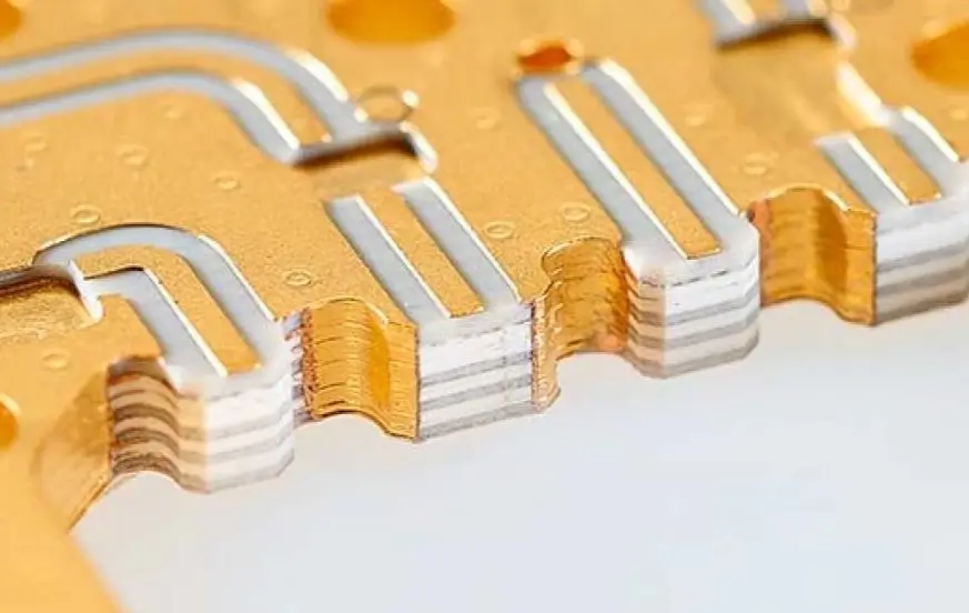
High-speed boards care about Impedance Control (usually ±10%). High-frequency boards, however, push the limits of physics. For 77GHz radar, line width tolerances must be within ±0.02mm. Even the "bumpiness" of the copper (Surface Roughness) matters—smooth signals need smooth copper, so we use Reverse Treated Foil (RTF) or HVLP copper.
When it’s time for "the physical":
- High-Speed Testing is like an eye exam. we look at Eye Diagrams to see if the signal "eye" is open wide enough for the receiver to read it.
- High-Frequency Testing is more like acoustic analysis. We use a VNA (Vector Network Analyzer) to check S-parameters—how much energy reflected back (S11) and how much made it through (S21).
6. Real-World Pitfalls: Lessons from the Lab
- 1. Don't be Fooled by Low Frequencies: A slow MCU clock can still have a super-fast rise time. If you don't match the impedance, your board will ring like a bell. Watch the edge, not just the frequency.
- 2. Teflon isn't a Magic Bullet: If you’re only working at 2.4GHz or 5GHz, standard high-performance FR-4 or Rogers 4003C is usually better and cheaper than pure PTFE.
- 3. Think System-Wide: Impedance isn't just about trace width. The pads on your connectors, the "stubs" on your vias, and even the size of your AC coupling capacitors are all potential signal killers.
7. Frequently Asked Questions (FAQ)
1. When should a PCB be considered “highspeed” rather than a normal board?
A PCB is considered “highspeed” when the signal rise/fall times and edge rates are fast enough that simple wiring assumptions break down and transmission line effects dominate. This means that impedance control, reflections, crosstalk, and timing skew all need to be managed during layout and stackup design. It’s not just about clock frequency — it’s about how fast the signal transitions relative to the trace length.
2. What is the real difference between “highspeed” and “highfrequency” PCB design?
Although the terms are sometimes used interchangeably, they have different design goals.
- Highspeed PCB design focuses on managing the integrity of fast digital signals, making sure that data arrives reliably without timing errors or degradation.
- Highfrequency PCB design focuses on preserving analog/RF signal energy, minimizing loss and distortion in radio, microwave, or millimeterwave signals. Highfrequency boards require stricter control of dielectric properties and signal loss over a wide frequency band.
3. How does material selection differ between highspeed and highfrequency PCBs?
Material choices differ because of the design priorities:
- Highspeed boards often use modified FR4 or other lowloss laminates that balance performance and cost. The goal is to keep signal distortion low and maintain controlled impedance for digital edges.
- Highfrequency boards use specialized substrates (like PTFEbased materials or ceramicfilled laminates) that offer very stable dielectric characteristics and low loss at RF and microwave frequencies. These materials tend to be more expensive and require more precise fabrication.
4. What layout strategies are key when designing highspeed vs highfrequency circuits?
The layout emphasis differs:
- In highspeed digital routing, designers focus on trace length matching, differential pair consistency, and uninterrupted reference planes so that timing and signal integrity are preserved.
- In highfrequency RF routing, the priority is precise transmission line geometry, short traces, minimal vias, and smooth transitions to reduce parasitic inductance and capacitance that degrade RF performance.
5. How do engineers verify performance for highspeed vs highfrequency boards?
Different validation approaches are used:
- For highspeed digital designs, engineers often rely on timedomain measurements such as eye diagrams and timedomain reflectometry to check for reflections, timing errors, and signal integrity issues.
- For highfrequency/RF boards, frequencydomain measurements like Sparameter analysis (e.g., with a vector network analyzer) are used to assess impedance matching, insertion loss, and return loss across operating frequencies.
Conclusion
High-speed and high-frequency design might share the same physics, but their methodologies are worlds apart. One is a race for logical certainty in a tiny window of time; the other is a quest for energy purity over a long distance.
A great PCB engineer knows how to calculate impedance—but a master knows how to find the sweet spot between cost, manufacturability, and performance.
This guide is based on IPC standards and industry best practices. Always validate your specific design with simulation and manufacturer feedback.
>>IPC-A-610 >>IPC-A-600 >>IPC 6012 >>IPC-2221
Optimize Your Design & Accelerate Production
Upload & Get Professional DFM Review Today Get Advanced PCB Capabilities at NextPCB
About the Author
Julia Wu - Senior Sales Engineer at NextPCB.com
With over 10 years of experience in the PCB industry, Julia has developed a strong technical and sales expertise. As a technical sales professional, she specializes in understanding customer needs and delivering tailored PCB solutions that drive efficiency and innovation. Julia works closely with both engineering teams and clients to ensure high-quality product development and seamless communication, helping businesses navigate the complexities of PCB design and manufacturing. Julia is dedicated to offering exceptional service and building lasting relationships in the electronics sector, ensuring that each project exceeds customer expectations.


 NextPCB Capabilities
 PCB Assembly
 Layer Buildup
 SMD-Stencils
 PCB Design-Aid & Layout
 Mechanics
 Surface
 Quality
 Drills & Throughplating
 Factory & Certificate