
 Surface


Stacy Lu

 NextPCB Capabilities
Printed Circuit Boards
NextPCB Capabilities
Printed Circuit Boards
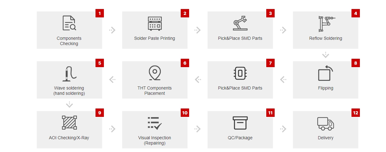
 PCB Assembly
 Layer Buildup
 SMD-Stencils
 PCB Design-Aid & Layout
 Mechanics
 Quality
 Drills & Throughplating
 Factory & Certificate
 PCB Assembly Factory Show
Certificate
PCB Assembly Factory Show
Certificate
Support Team
Feedback:
support@nextpcb.com


Introduction
In the precision world of PCB manufacturing, a simple "mirroring" error can be catastrophic. Imagine waiting for a quick turn PCB order to arrive, only to discover that the bottom layer text is backward, or worse, the footprint for a 144-pin FPGA is mirrored. The board is unbuildable. The components won't fit. The time and money are lost.
Layer orientation (often called layer labeling) is the critical communication bridge between your EDA design software and the CAM engineers at the fabrication house. While modern manufacturing has advanced significantly by 2026, correct copper labeling remains the only fail-safe method to ensure your design intent is perfectly understood.
This guide dives deep into technical best practices for layer orientation, helping you streamline your Design for Manufacturing (DFM) process and ensure seamless PCB assembly.
Incorrect or missing layer labels are one of the most common causes of engineering holds (EQ) in the industry. When a manufacturer receives Gerber files without clear orientation markers, they face a dilemma:
Many layout programs allow for "mirrored output" when generating Gerbers. If a designer accidentally checks a "Mirror" box during export, the machine reads the data effectively "upside down." Without a physical text marker etched into the copper, there is no reference point to correct this.
To master layer orientation, you must understand how manufacturers view your data. Whether you are designing a simple 2-layer board or a complex HDI rigid-flex, standard Gerber data is processed using a "View from Top" perspective.
This means:
If you view your Gerber files and the text on the bottom layer is readable from left to right, your board will likely be fabricated incorrectly (mirrored), rendering through-hole and SMT footprints unusable.
Let's look at a common scenario encountered by our CAM engineers at NextPCB. The image below shows a copper layer export with no text labels.

Figure 1: Can you tell if this is a top or bottom layer? Without labels, it is impossible to be 100% sure.
Even if the file name is project_name.GBL (Gerber Bottom Layer), software glitches or user export errors can result in the data being flipped. Without an etched label like "TOP" or "BOT" integrated into the copper traces, the manufacturer cannot verify if the geometry is correct relative to the physical board stack-up. This ambiguity is a primary risk factor in low cost PCB production where automation is high.
The industry standard for eliminating ambiguity is simple: Write it in the copper.
Placing text in the silkscreen is helpful, but Silkscreen is printed after solder mask and etching, so it cannot be used as a reliable manufacturing reference. Copper features are etched first. By placing text in the copper, you provide an immutable reference point for the entire fabrication process.
As shown in the example below, the "TOP" label is readable, and the "BOT" label is mirrored. This confirms the file adheres to the standard "View from Top" convention.

Figure 2: Correct orientation. "TOP" is readable; "BOT" is mirrored in the design view.
When the physical board is produced and you flip it over to look at the bottom, that mirrored "BOT" text will appear legible to the human eye. If it is legible in the design software, it will be backward on the physical board.
Modern formats such as Gerber X2 and ODB++ include embedded layer attributes, which significantly reduce orientation ambiguity. However, copper text labeling is still considered best practice as a physical, fail-safe verification method.
For multilayer boards, the risk increases. An inverted inner layer can cause short circuits between power and ground planes or connect signals to the wrong nets. This is impossible to fix after lamination.
For turnkey PCB projects involving complex stacks, we recommend a "staircase" labeling method in the border area of the panel or the board edge.

Figure 3: Sequential labeling for Inner Layers (L1, L2, L3, L4).
Standard Protocol for Multilayers:
Layer orientation doesn't just affect the bare board; it dictates the success of the PCBA (Printed Circuit Board Assembly) process.
If a Bottom Layer is mirrored during fabrication:
Detecting this error at the assembly stage is devastating because the bare boards must be scrapped, and components may have already been wasted. At NextPCB, our automated optical inspection (AOI) checks for these issues, but correct data input is paramount.
Before you generate your Gerber X2 or ODB++ files, run through this quick checklist to ensure your quick turn PCB order goes smoothly:
Yes. Since you are viewing the board "through" the substrate (X-ray view) in most EDA tools (Altium, Eagle, KiCad), text on the bottom layer should appear backward (mirrored) on your screen. This ensures it reads correctly when you hold the physical board.
Yes. Our CAM engineers perform a detailed Design for Manufacture (DFM) review. If we see text that is unreadable or conflicting orientation, we will put the order on "Engineering Hold" and contact you. However, to ensure the fastest delivery for quick turn PCB services, correct labeling prevents these delays.
While file names are the first indicator, they are not foolproof. Software settings can accidentally mirror the data inside a correctly named file. Physical copper labels are the only 100% verification method.
Inner layers should be numbered sequentially (L2, L3, etc.). Generally, inner layers are viewed as "positives." Ensure the numbers are positioned so they don't overlap when viewing the board as a composite, allowing for easy stack-up verification.
At NextPCB, every order goes through automated CAM checks and manual engineering review to catch orientation risks before fabrication.
Still, clear copper labeling is the fastest way to avoid delays and keep your quick-turn schedule on track.

Still, need help? Contact Us: support@nextpcb.com
Need a PCB or PCBA quote? Quote now

