Stacy Lu

Support Team
Feedback:
support@nextpcb.comTable of Contents
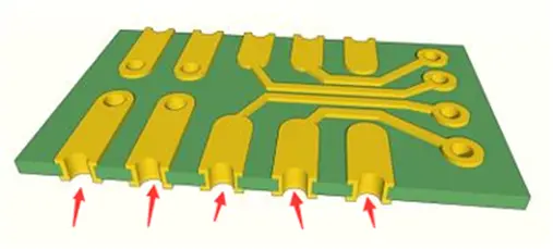
Plated half-holes, commonly referred to in the engineering community as castellated holes, side plating, or edge plating, are plated through-holes (PTH) located directly on the boundary (outline) of a printed circuit board. During the final routing stage of PCB manufacturing, these holes are intentionally bisected. The resulting edge of the PCB resembles a series of half-cylinders lined with copper plating, looking much like the battlements of a medieval castle.

By transforming the edge of a board into a robust connection interface, castellated holes allow one printed circuit board to be mounted directly flush onto another larger motherboard. This board-on-board connection technique has become increasingly vital as hardware designs shrink and modular architectures dominate modern electronics.
As we navigate through the hardware trends of 2026, modularization is at its peak. Hardware developers prefer designing standardized sub-modules that can be attached to various mainboards. Plated half-holes are the cornerstone of this design philosophy.
Beyond electrical connectivity, plated half-holes serve a critical role in thermal management for high-power modules. In modern high-current DC-DC converters or LED driver modules, the half-holes act as a direct thermal path to the motherboard's ground planes. Because the copper barrel of the half-hole is soldered directly to a large landing pad on the carrier board, it creates a low-resistance conduit for heat transfer. This auxiliary cooling mechanism helps maintain lower junction temperatures for power ICs mounted on the daughterboard.
Standard routing will destroy a plated half-hole. To produce clean, reliable results, NextPCB utilizes a specialized workflow: Primary Drilling → Copper Plating → Specialized Edge Routing → Chemical Deburring. This ensures no copper shards remain, preventing shorts during the PCBA stage.
Properly defining castellated holes in your Gerber files is critical. To ensure structural integrity and prevent copper delamination during fabrication:
In volume production, panelization is key. However, half-holes are fragile. At NextPCB, we recommend using Tie-bars (connection joints) strategically placed away from the castellated areas. If a module is surrounded by half-holes on all four sides, use a "bridge" or "post" design on the corners. This prevents the depaneling force (V-scoring or Tab-routing) from stressing the copper plating in the holes, ensuring that the sidewalls remain intact and burr-free for assembly.
The ENIG Advantage: For castellated boards, ENIG (Electroless Nickel Immersion Gold) is the gold standard. Unlike HASL, ENIG provides:
NextPCB utilizes optimized routing vectors and strict quality control checks to eliminate copper peeling. We offer comprehensive turnkey PCB assembly solutions that consider the unique soldering requirements of castellated modules.
| Specification | Standard Capability | Advanced Capability |
|---|---|---|
| Min Hole Diameter | 0.5 mm | 0.3 mm (Custom) |
| Min Annular Ring | 0.15 mm | 0.12 mm |
| Min Distance Between Holes | 0.55 mm | 0.50 mm |
Castellated holes are individual bisected holes used for pad-to-pad soldering. Edge plating (or side plating) involves plating the entire length of a board's edge for EMI shielding or grounding. While they share similar manufacturing techniques, castellated holes are functional signal/power interconnects.
Yes. By increasing the number of half-holes and ensuring a robust annular ring, they can handle significant current. They also act as a thermal path to dissipate heat from high-power components.
ENIG provides a flat surface and prevents the sidewalls of the half-hole from oxidizing. HASL can result in uneven solder thickness, leading to "tombstoning" or poor alignment during the PCB module soldering process.
Use Tie-bars or connection tabs placed at the corners of the board, rather than directly on the edges with the half-holes. This ensures the routing/snapping forces do not damage the delicate copper plating within the holes.
Still, need help? Contact Us: support@nextpcb.com
Need a PCB or PCBA quote? Quote now