Zhang

Support Team
Feedback:
support@nextpcb.comIn the world of electronics manufacturing, the transition from a prototype design to mass production hinges on one critical factor: efficiency. While a single Printed Circuit Board (PCB) might work perfectly on a test bench, it is often too small, too irregular, or too unstable to travel through the automated conveyor rails of modern SMT (Surface Mount Technology) assembly lines.
As we advance into 2026, where component miniaturization (01005 packages and smaller) and high-density interconnects (HDI) are standard, the precision of your PCB panel design is more critical than ever. A poorly designed panel can lead to board warping during reflow, component cracking during depaneling, or excessive material waste that drives up your low cost PCB targets.
This guide explores the engineering mechanics of panelization, comparing V-Scoring and Tab-Routing, and provides actionable DFM (Design for Manufacturability) advice to help you optimize your PCB manufacturing and PCB assembly processes with NextPCB.
Panelization—also known as stepping, palletization, or array—is the process of arranging multiple individual PCB units onto a larger substrate. This isn't just about handling; it's a strategic move for turnkey PCB projects.
Modern Pick and Place machines are marvels of automation, capable of placing components at speeds exceeding 100,000 cph (components per hour). However, every time the machine has to load a new board and align its cameras (fiducial recognition), valuable seconds are lost.
By panelizing 6 or 12 units together, the machine loads once and assembles continuously. This significantly boosts the utilization rate of the SMT line, reducing the overall PCBA labor cost and shortening lead times for quick turn PCB orders.
PCB laminates (FR4, Rogers, Aluminum) come in standard sheet sizes. Designing a panel that nests odd-shaped boards can increase board utilization by 15-30%. Less waste material means a lower price per unit.
Small boards are lightweight and prone to shifting during the solder paste printing process. A panel with a sturdy waste frame (break-away rail) adds rigidity, ensuring flatness during the thermal shock of the reflow oven.
There are two primary industry standards for connecting individual boards within a panel. The choice depends heavily on your board's outline and component proximity to the edge.
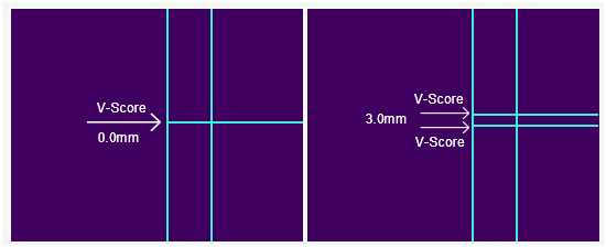
V-scoring involves cutting a "V" shaped groove from both the top and bottom of the PCB, leaving a thin layer of material intact to hold the boards together.
Figure 1: Typical V-Cut panel layout showing zero spacing between units.

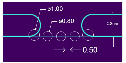
For PCBs with irregular shapes, we use a CNC router to mill out the board outline, leaving small tabs.
Figure 2: Perforated tabs (Mouse Bites) allow for controlled breaking points.

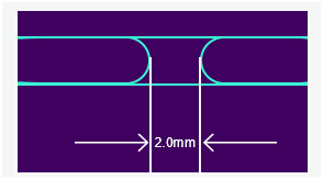
Solid tabs are used when the panel needs maximum rigidity or when using specialized router machine depanelers.
Figure 3: Solid tabs provide rigidity but require mechanical cutting.

As components shrink to 01005 and 008004 sizes, even the slightest mechanical vibration from a V-cut snap or a CNC router can cause solder joint micro-cracks.
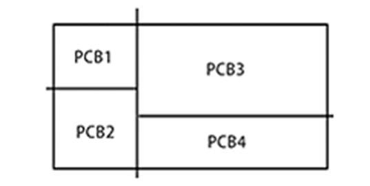
Laser Depaneling is now the preferred hybrid choice for high-end PCBA. In a hybrid setup, the board might be V-scored for bulk material removal and then Laser-cut near sensitive components or complex flex-circuit transitions. Laser cutting is stress-free, leaves no carbonization (with UV lasers), and allows for much tighter component-to-edge clearances.
Figure 4: Irregular shapes like circular LEDs require tab-routing or laser cutting.

Use the following table to verify your panel design before submission to NextPCB.
| Feature | Requirement | Design Purpose |
|---|---|---|
| Process Rails | 5mm - 7mm (Min) | Conveyor rail clearance for SMT machines. |
| Fiducial Marks | 1.0mm (Copper) + 2.0mm (Clearance) | Optical alignment for Pick & Place precision. |
| 3.05mm (Non-Plated) | Secures board in test fixtures and Wave Solder pallets. | |
| Component Keep-out | 3.0mm from Tab / 1.0mm from V-Cut | Prevents stress-induced cracking (especially for MLCCs). |
| Copper Thieving | Solid or Dot Pattern in rails | Balances copper density to prevent board warping in reflow. |
One of the most overlooked aspects of DFM is mechanical stress. Snapping a board by hand is never recommended for professional PCB assembly.
Warning: Ceramic capacitors (MLCCs) are extremely brittle. NextPCB recommends using a "V-Cut Saw" or "Laser Depaneler" instead of manual snapping to maintain the integrity of 0402 and 01005 components.
At NextPCB, we specialize in high-reliability fabrication. Our 2026 standards include:
Pro Tip: Select "Panel by Manufacturer" when using our online quoting tool. Our CAM engineers will optimize your panel for the best material utilization, often reducing your turnkey PCB costs significantly.
A: Choose V-cut for rectangles to save space. Choose Tab-route for irregular shapes or if you have components hanging over the board edge.
A: No. All boards in a single panel must share the same stack-up, material, and copper thickness.
A: In mass production, NextPCB marks defective units on a panel with an "X". Modern SMT machines read these marks and skip the bad board, ensuring no expensive components are wasted.
NextPCB ensures your boards are built to the highest 2026 industry standards. Our engineers review every file for potential DFM issues before production begins.
Still, need help? Contact Us: support@nextpcb.com
Need a PCB or PCBA quote? Quote now