Lolly Zheng- Sales Account Manager at NextPCB.com

Support Team
Feedback:
support@nextpcb.comIn the world of electronics manufacturing, efficiency is currency. PCB Panelization (also known as creating a "PCB array") is a fabrication technique where multiple smaller circuit board units are arranged and connected on a single larger substrate (the "panel") to be processed simultaneously.
While prototyping often involves single boards, mass production almost always requires panelization. Why? Because moving 50 individual small boards through an SMT (Surface Mount Technology) assembly line is slow and prone to error. Moving one panel containing 50 boards is fast, stable, and cost-effective. Unless your PCB is exceptionally large or requires specialized processing, NextPCB always recommends designing a panel to maximize throughput and yield.
Understanding panel utilization is crucial for procurement managers and engineers aiming for low cost PCB production. PCB laminates typically come in standard manufacturing sheet sizes (e.g., 18" x 24"). The goal is to fit as many boards as possible onto these sheets with minimal waste.
From a fixed panel cost, increasing the number of boards packed into one panel directly lowers the price per unit. However, geometry plays a massive role here. Simply rotating a board can dramatically change the yield.
Consider the example below involving identical PCBs. By analyzing the dimensions, we can see how orientation impacts density:
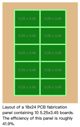
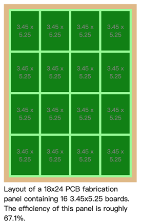
The Analysis: In the comparison above, simply rotating the boards 90 degrees allows for 60% more boards on the same panel size. This is a classic example of DFM (Design for Manufacturability) optimization. Professional PCB fabricators like NextPCB will usually optimize this for you during the engineering query (EQ) phase, but providing a pre-optimized array design ensures you get the most accurate quote upfront.
Depending on your project needs, panels generally fall into two categories:
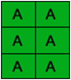
This consists of identical PCB designs repeated across the panel. This is the industry standard for mass production, allowing for high-speed turnkey PCB assembly and simplified inventory management.
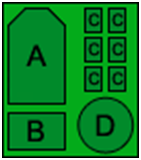
This method combines different PCB designs (e.g., a mainboard and a daughterboard) onto a single panel. This is often called a "family panel."
V-scoring involves cutting a triangular groove into the top and bottom of the PCB. The boards are snapped apart after assembly.
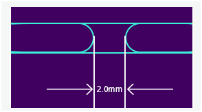
For irregular shapes, we use routing with "Mouse Bites" (perforated tabs).
| Feature | V-Scoring (V-Cut) | Tab-Routing (Mouse Bites) |
|---|---|---|
| Applicable Shapes | Rectangular / Straight lines only | Any shape (Circular, Irregular) |
| Edge Quality | Rougher, V-shaped slope | Smooth, but with small bumps (Tabs) |
| Material Utilization | Very high (0mm spacing) | Lower (1.6mm - 2.0mm gap required) |
| Depanelization Ease | Easy (Manual or Scorer machine) | Moderate (Requires cutters or router) |
To support high-speed 2026 SMT standards, your panel requires a process frame:
Large panels or panels with thin PCBs (< 1.0mm) are prone to bending (warpage) during the high temperatures of reflow soldering. For 2026 high-density designs, NextPCB recommends adding stiffeners or internal rails if the panel width exceeds 200mm to ensure flatness and prevent solder defects.
In high-volume manufacturing, it is common for one or two units in a panel to fail electrical testing.
Mouse bites should never be placed near high-stress zones. Breaking the tabs generates vibration; if placed too close to a ceramic capacitor or a BGA, it can lead to latent micro-cracks in the components.
Rigidity refers to how well the panel resists bending. If your board has heavy components like power modules, the panel may sag during soldering. In such cases, we suggest wider process rails or increasing the PCB thickness.
If your PCB must fit into a tight enclosure, design the mouse bites to be "recessed" within the board edge. This way, the breakout nub stays inside the board's boundary rather than protruding outwards.
Yes. Our DFM (Design for Manufacturability) check includes verifying clearances. If we find internal copper too close to a V-cut line (risking shorts), we will raise an Engineering Query (EQ) before production.
With over 15 years of industry experience and state-of-the-art intelligent manufacturing, NextPCB handles the complexities of fabrication so you can focus on design.
Need help with your panel layout?
Still, need help? Contact Us: support@nextpcb.com
Need a PCB or PCBA quote? Quote now