
 NextPCB Capabilities
Printed Circuit Boards
NextPCB Capabilities
Printed Circuit Boards
 PCB Assembly
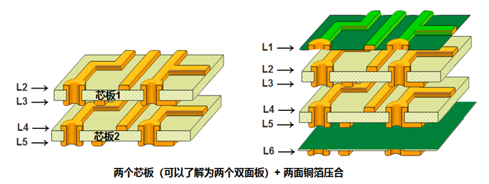
 Layer Buildup
 SMD-Stencils
 PCB Design-Aid & Layout
 Mechanics
 Quality
 Drills & Throughplating
 Factory & Certificate
 PCB Assembly Factory Show
Certificate
PCB Assembly Factory Show
Certificate
Support Team
Feedback:
support@nextpcb.com


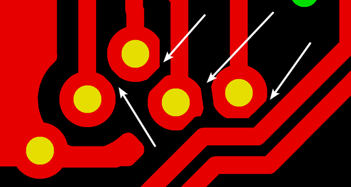
When designing the PCB board, the most consideration for our wiring is how to connect each layer to the network signal line in the most reasonable way. The denser the high-speed PCB board circuit, the greater the density of vias (VIA) is placed, and the vias can serve each layer. The role of electrical connection between.
Multi-layer circuit board PCB proofing often receives feedback from the board manufacturer "the hole is too close to the line, which exceeds the process capability", so what difficulties will there be for production if the vias are too close, and what impact does it have on product reliability?
For the following six-layer PCB, the inner hole edge to the line edge is 6 mil, the hole is 4 mil, and the ring to the line is only 2 mil (Figure 1). The effect after cutting the pad (Figure 2).

Why Choose NEXTPCB Manufacturer
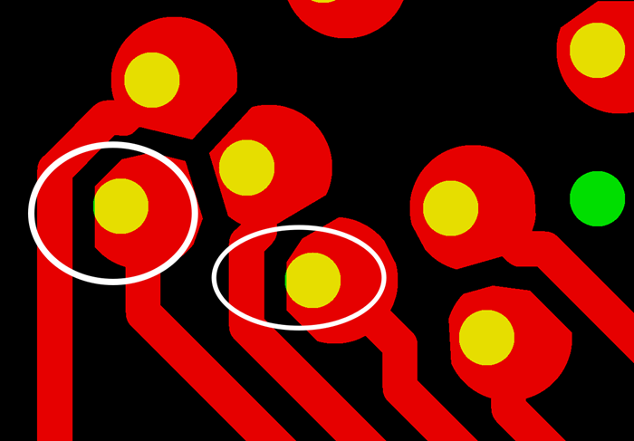
In summary, the drilling process affects the PCB yield rate and PCB production efficiency. There is no complete copper protection around the hole ring via the small hole, and the PCB open and short circuit test can pass, and there will be no problems in the early use of the product, but the long-term use reliability is not enough.
NEXTPCB recommends that the multi-layer PCB board, high-speed PCB board hole-to-hole, hole-to-line spacing:
(1) The inner layer of the multilayer board from the hole to the wire to the copper:
(2) The edge spacing of the inner diameter of the via:
Still, need help? Contact Us: support@nextpcb.com
Need a PCB or PCBA quote? Quote now


 Surface

