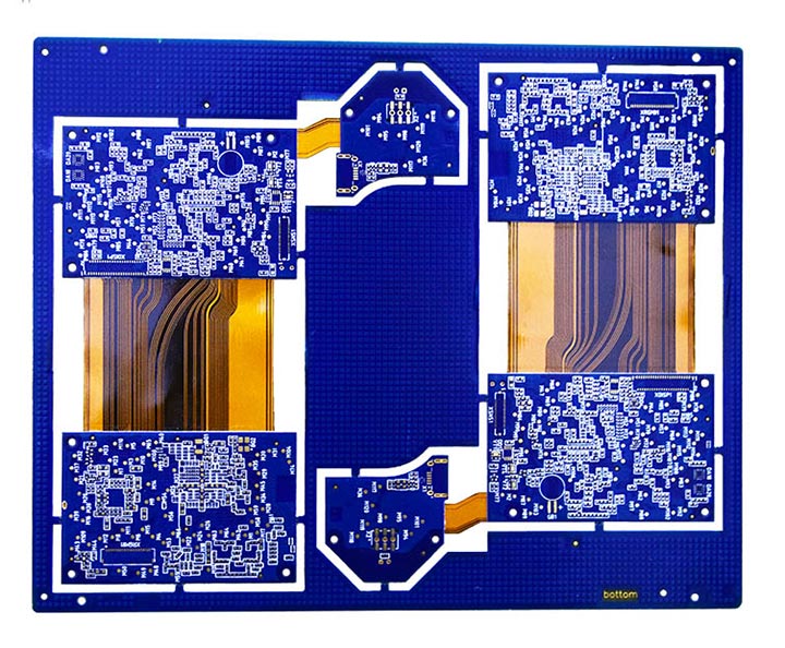
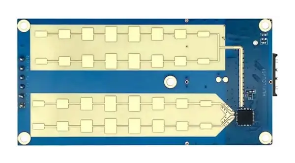
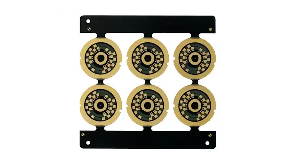
A rigid-flex PCB is a printed circuit board that seamlessly integrates both rigid and flexible regions into a single interconnected unit. By combining these two distinct mechanical properties, rigid-flex boards leverage the best of both worlds: the high density and reliability of rigid boards, alongside the dynamic deformation and spatial adaptability of flexible boards.
Whether in space-constrained medical electronics, wearable devices, or aerospace and military systems demanding extreme fault tolerance, rigid-flex boards deliver innovative interconnect solutions that break through the physical limitations of traditional PCBs.
At NextPCB, we provide precision rigid-flex PCB manufacturing and assembly services for compact and dynamic devices spanning medical electronics, wearables, aerospace, and other fail-safe systems. Whether you are looking for the space-saving benefits or the signal integrity advantages of rigid-flex structures, our rigid-flex solutions will drive innovation and push beyond the boundaries of conventional PCBs.
I. Why Choose Rigid-Flex PCBs? Core Advantages & In-Depth Design Details
In various applications, rigid-flex boards unlock numerous advantages over standalone rigid boards, flex boards, or cable interconnect designs. To maximize these benefits, engineers must master specific technical details during the design phase.
1. Extreme Component and Routing Density
Rigid-flex boards utilize rigid sections to achieve incredibly high component and signal density. Compared to rigid assemblies using discrete flexible cables or all-flex designs, they enable much more compact and lightweight systems.
- Components and traces can be packed much tighter than in pure flex PCBs.
- The rigid sections can accommodate higher layer counts without compromising the system's overall flexibility.
- They can leverage complex HDI (High-Density Interconnect) structures, such as blind/buried vias and microvias, to further reduce board size and weight.
- Bulky on-board flex connectors and cable pads are completely eliminated.
2. Superior System Reliability and Stress Management
Thanks to their all-in-one integrated design, rigid-flex boards drastically reduce potential points of failure. Traditional connectors and wires can loosen over time, and solder joints can crack. By eliminating these elements, rigid-flex designs are exceptionally well-suited for harsh environments subject to high vibration and frequent bending.
Deep Engineering Design Tips: Combating Stress Concentration
- Anti-Fracture Routing Rule: Flex regions are highly susceptible to stress concentration. During the layout phase, traces passing through the flex area and the rigid-flex transition zone must strictly avoid 90-degree or 45-degree sharp corners; circular arc routing is mandatory.
- Tear-dropping: All via and pad connections in the flex region should incorporate teardrops to smooth the transition cross-section, preventing the connections from tearing under dynamic bending stress.
- Transition Zone Stress Management: The physical boundary between the rigid and flex regions (the Transition Zone) is the most vulnerable part of the entire board. When designing, ensure a "no-via routing zone" of at least 1-2mm at the boundary. Additionally, strategically place stiffeners (such as PI or FR4 materials) to shift the bending stress point away from the physical rigid-flex edge, allowing for smooth stress dissipation.
3. Optimized Signal Integrity and Ground Plane Design
Connectors are inherently impedance-discontinuous interfaces that introduce reflections and noise, degrading high-speed signals. By eliminating cable connectors and utilizing materials with uniform structural and electrical characteristics, managing noise, crosstalk, and impedance discontinuities becomes significantly easier.
Deep Engineering Design Tips: Balancing Mechanical Flexibility and Electrical Performance
- Avoid "Solid Copper Ground" in Pure Flex Zones: In pure rigid PCBs, a solid copper ground plane is the gold standard for signal integrity. However, laying large areas of solid copper foil in the flexible regions of a rigid-flex board creates a fatal "I-beam effect." The solid copper acts like the web of an I-beam, drastically increasing the physical stiffness of the area, making it highly prone to mechanical fatigue and copper foil fractures under repeated bending.
- Crosshatch/Mesh Planes: In flexible regions, using a 45-degree crosshatch ground plane is highly recommended. While this alters the effective dielectric constant and complicates impedance control calculations, it is the most reliable compromise between maintaining high-speed signal "impedance matching" and preserving the board's "dynamic bending lifespan."
4. Simplified Assembly and Testing Processes
Compared to standard flex PCBs, rigid-flex designs are easier to fabricate and assemble because: 1) The rigid sections keep the PCB flat and taut within the panel during manufacturing, and 2) Electronic components are typically populated on the rigid areas, while the flex sections handle signal transmission and bending, reducing alignment issues during PCB assembly and enhancing overall reliability. Although mounting fixtures may still be required to protect the flex segments from thermal damage (overheating) during assembly, the overall process is generally much simpler.
The absence of flex connectors and wiring also helps reduce manual installation labor and Bill of Materials (BOM) costs, especially for systems requiring high-pin-count or high-reliability connectors.
II. Disadvantages, Cost Drivers, and Cost-Reduction Strategies
1. High Upfront Costs and Material Expenses
Even for simply designed rigid-flex PCBs, manufacturing costs are quite high. Because each stackup is intricately tied to the specific performance and functionality of the design, it is difficult to panelize multiple different designs together for manufacturing (making standard pooled prototyping services unavailable). This keeps the prototyping costs for rigid-flex boards inherently high, making them less viable for one-off applications.
Cost Analysis and Cost-Down Strategies:
- Raw Material Costs: In the total cost of a rigid-flex board, specialized raw materials (such as polyimide and dedicated adhesive sheets) typically account for 20% to 60%.
- Avoid "Over-specifying": Engineers should avoid over-specifying expensive, specific material brands in the BOM. As long as the material parameters meet the peel strength, dimensional stability, and thickness tolerances defined in IPC-4203 (Coverlay standard), allowing the manufacturer some flexibility in material substitution can significantly drive down costs.
- Optimize Panelization: Flex regions often feature irregular shapes. Considering the factory's panel layout early in the design phase and improving material utilization through a "nesting" approach can drastically reduce the per-unit price.
> Learn More Cost-Down Strategies: 6 Cost Mistakes to Avoid for Lower PCB Cost & Overheads
2. Difficult to Repair
While boards connected via discrete cables have more points of failure, these points are usually easy to fix. Broken connectors, snapped cables, or even damaged pads can be replaced, and solder joints can be reworked. However, if a rigid-flex PCB suffers a tear in the flex region or an internal broken trace, it is almost impossible to repair without destroying the entire unit, which typically means the whole PCBA must be scrapped. Unless specialized tools and expertise are utilized, the entire assembly usually requires replacement. This difficulty in repair is a primary reason why you rarely see rigid-flex designs in cost-sensitive consumer electronics.
III. When Should You Choose a Rigid-Flex PCB for Your Design?
Despite their many advantages, rigid-flex PCBs are not a practical solution for every multi-board application.
High tooling costs, upfront expenses, and repair difficulties restrict rigid-flex designs primarily to applications where reliability and failure prevention are the main decision drivers, such as aerospace, military, or medical devices. Alternatively, they are chosen in high-speed designs where a rigid-flex structure is strictly necessary to maintain signal integrity.
Considering the high component density and manufacturing expenses, the upfront costs make prototyping rigid-flex designs expensive. They are generally unsuitable for one-off projects, highly cost-conscious designs, or applications requiring field-repairable, easily recoverable units.
IV. Advanced Construction Types & IPC Material Standards
For applications with extreme space constraints, standard rigid-flex stackups often fall short. Engineers need to understand more advanced construction techniques:
- Bookbinder Construction: For extremely high-density designs requiring multiple layers to fold within a confined space, the inner and outer layers follow different bend radii. The bookbinder construction utilizes precise calculations to make the inner flex layers shorter and progressively lengthen the outer flex layers (adding bend allowance)—much like the spine of a book. This completely eliminates wrinkling and internal stress when multi-layer flex boards are bent.
- Bikini Build: This is a specialized coverlay treatment process where the coverlay does not span the entire board; instead, it only "partially" extends into the rigid region. This effectively reduces the overall thickness of the rigid section and mitigates the risk of delamination (board pop) caused by stacking multiple materials with drastically different Coefficients of Thermal Expansion (CTE).
V. Design for Manufacturability (DFM) & Factory Processing Challenges
To ensure a smooth transition to mass production, understanding the manufacturing challenges at the factory level is critical for an engineer's DFM assessment:
- Layer-to-Layer Registration: Rigid-flex boards incorporate various materials (FR4, PI, acrylic adhesives, etc.) that shrink at different rates under temperature and pressure. Maintaining extreme layer-to-layer alignment accuracy across multiple lamination cycles is a core challenge. During design, engineers should appropriately increase the tolerance margins for pads and annular rings at the rigid-flex junctions.
- Back-drilling for High-Speed Signals: In high-speed rigid-flex applications, if a signal transitions to a shallower layer via a through-hole, the leftover via stub can severely degrade signal integrity. Factories must precisely remove these stubs using a back-drilling process, which demands exceptionally tight depth-control capabilities for rigid-flex boards.
- Automated Material Handling: Because flexible materials are inherently thin and fragile, they are highly prone to jamming or wrinkling during processes like drilling and plating. Selecting a manufacturer equipped with automated flexible material handling and transfer systems is key to ensuring high yields and consistent quality in high-volume production.
VI. NextPCB Rigid-Flex PCB Manufacturing Capabilities
NextPCB supports the custom manufacturing and assembly of rigid-flex printed circuit boards, accommodating up to 32 rigid layers and 6 flex layers. We feature advanced stackups and configurations that comply with stringent international standards, including ISO9001:2015, IATF16949, ISO13485, and IPC-6013 Class 3, complete with impedance testing and support. Choose NextPCB to deliver reliable results for your mission-critical products.
| Feature |
Rigid |
Flex |
| Circuit Layers |
2 to 32 layers |
1 to 6 layers |
| Base Material |
FR4 |
Polyimide (PI) |
| Covering Type |
Solder mask |
PI coverlay or flexible solder mask |
| Surface Finishes |
ENIG, OSP and Immersion silver |
| ENIG Gold Thickness |
1 to 3μ" |
| PCB Thickness |
0.4 to 3.2mm |
0.1 to 0.45mm |
| Copper Thickness |
1 to 6 oz |
1/3 to 1 oz |
| Min. Trace width/spacing |
3/3 mil |
2/2 mil |
| Min. Drill Hole Diameter |
0.1mm |
| Solder Mask/Coverlay Color |
Solder Mask: Green, red, yellow, orange, black, silver and clear |
Coverlay: Yellow, white, black and clear |
| Extras |
- HDI Structure
- EMI shielding
- Impedance control
- Filled & capped vias
- Stiffeners see flex PCBs
- Laser or mold forming
- Conductive adhesive
- 3M adhesive backing
- And more
|
Ready to validate your design 2026?
[Upload your Gerber files] for a free 24-hour DFM review
Or inquire for advanced capabilities.
VII. Rigid-Flex PCB Technical FAQs
Q1: Since rigid-flex boards are so superior, why are quotes usually several times more expensive than a "rigid board + cable" solution?
A: This is primarily due to many "invisible operations" hidden within the manufacturing process. Rigid-flex boards require multiple lamination cycles, and the flexible layers (Polyimide) shrink and deform under high temperatures. To guarantee alignment precision down to a few microns for every layer, the scrap rate is much higher than that of standard boards. Additionally, applying the specialized coverlay is often a time-consuming, highly manual process.
Q2: How exactly should the Bend Radius be calculated to prevent the copper foil from breaking?
A: The standard industry guidelines are:
- Static Bending (bent once during installation): Radius ≥ 10 times the total thickness of the flex region.
- Dynamic Bending (continuously folding during operation): Radius ≥ 20 times the total thickness.
- Note: Absolutely never place vias directly on the bend, nor allow traces to switch layers at the bend. These are the most vulnerable points for fracturing.
Q3: Why can't the standard liquid photoimageable solder mask (green oil) be used on the flexible sections?
A: Traditional solder mask becomes brittle once cured and will crack immediately upon bending. The flexible regions must use a Coverlay. This is a polyimide film with an adhesive backing that is applied over the circuit like a sticker. Although more expensive, it bends seamlessly with the circuit without cracking.
Q4: What are the default design rules for the transition zone (the boundary between rigid and flex)?
A: This is the most failure-prone area. You must adhere to the following rules when designing:
- Perpendicular Traces: Traces must enter the rigid zone perpendicular to the transition boundary.
- Teardrop Reinforcement: Traces entering pads or crossing the transition boundary must include "teardrops" to disperse stress.
- Keep Vias Away: Vias must be placed at least 1mm away from the transition line; otherwise, the extrusion stress during lamination will tear the via barrel.
Q5: What is a "Hatched Ground," and why should it be used?
A: If you lay down a large area of solid copper foil in the flex region, the board will become as stiff as a steel plate. Converting the copper foil into a crosshatch (mesh) pattern ensures adequate electromagnetic shielding and signal integrity while allowing the board to retain excellent flexibility.
Q6: Why did my double-layer flex design break after only a couple of bends?
A: Check if your traces are overlapping. If you route the top-layer and bottom-layer traces directly on top of each other, it creates an "I-beam" effect, making the flex region extremely stiff and highly prone to snapping. The correct approach is to use Staggered Traces, arranging the top and bottom traces alternately so they avoid each other, much like the teeth of a zipper.

 NextPCB Capabilities
 PCB Assembly
 Layer Buildup
 SMD-Stencils
 PCB Design-Aid & Layout
 Mechanics
 Surface
 Quality
 Drills & Throughplating
 Factory & Certificate