
 NextPCB Capabilities
Printed Circuit Boards
NextPCB Capabilities
Printed Circuit Boards
 PCB Assembly
 Layer Buildup
 SMD-Stencils
 PCB Design-Aid & Layout
 Mechanics
 Quality
 Drills & Throughplating
 Factory & Certificate
 PCB Assembly Factory Show
Certificate
PCB Assembly Factory Show
Certificate
Support Team
Feedback:
support@nextpcb.com


For tasks that are still in the prototyping stage, it can be beneficial to have actually the vias revealed to be able to deal with as well as reroute traces, as well as be made use of as unplanned examination factors.
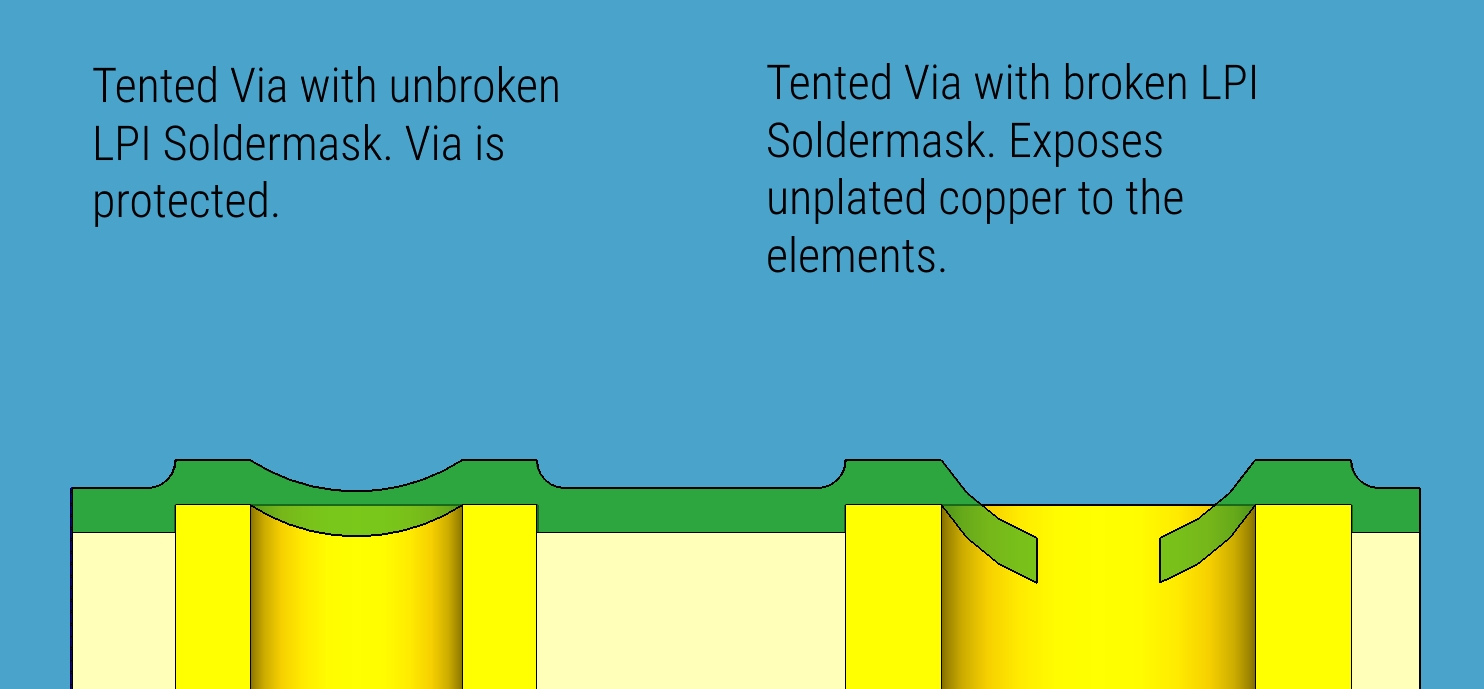
The duty of the PCB's solder mask is to shield the copper traces from damages, oxidation, and also solder connecting. These securities likewise put on the vias. Tented vias will certainly be a lot more immune to physical damages as well as electric shorts. If your PCB layout has through-hole elements that will certainly be wave firm after that a tented by means of will certainly avoid the solder from moving up right into the using and also over the opposite of the PCB where it can possibly short out parts. Vias that are likewise near to SMT pads need to additionally be tented. This will certainly stop the solder paste from wicking right into them.
by means of as well as producing an inadequate solder joint. This is particularly crucial with dogbone design BGA running away.
Tenting vias does have its disadvantages. Considering that the LPI solder mask is fluid, it needs to "bridge" the void over the by means of opening. This can trigger the solder mask to not totally outdoor tents the using leaving a tiny opening. The little opening can offer a method for harsh change, wetness, as well as various other chemicals to go into the using being entrapped. This can allow the opportunity of a failing of the by means of as a result of rust consuming the copper by means of. This is much less of a concern because of the appeal of no tidy change for SMT setting up yet harsh water tidy change is still widespread via opening setting up.
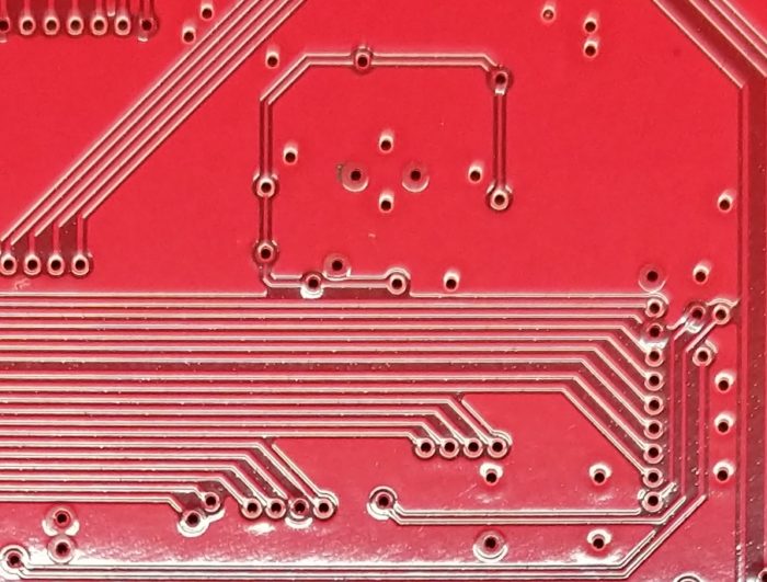
Leaving the vias revealed without a solder mask does not indicate the copper will certainly be open to the setting. The revealed vias will certainly be layered by the surface area coating of the PCB. At MacroFab we utilize the ENIG surface which will certainly cover the within subjected vias with gold, securing the copper from rust and also damages.
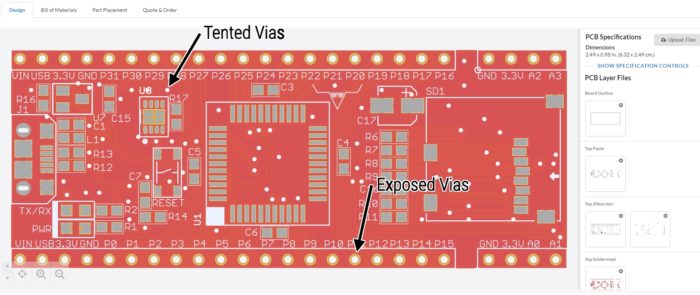
The PCB user interface on the MacroFab system supplies a simple means to examine the vias in your style to see if they are tented or otherwise. Just publish your layout data as well as examine the PCB provide. Tented vias will certainly reveal as simply the drill openings with solder masks covering the copper. Subjected vias will certainly have the solder mask pushed back from the annular ring by means of revealing the ENIG surface in the PCB makes.
PCB Design Analysis Software-NextDFM
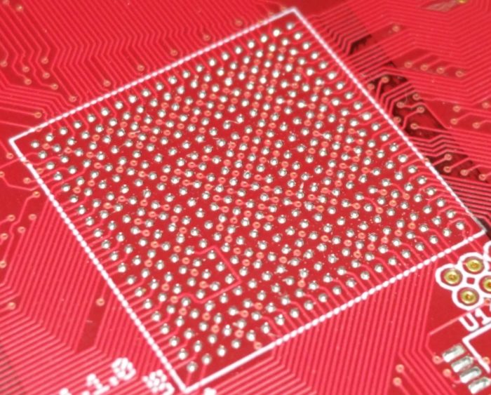
So should you outdoor tents your vias, or otherwise? For long-term dependability of the PCB, and also enhanced manufacturability of the PCB, it is far better to secure them by means of totally to avoid the access of dampness as well as liquids. Doing this financially can be a trouble. Loading vias with epoxy as well as covering (to be discussed in a future post!) can be pricey. Whether tenting a by means of with LPI solder mask can be done dependably depends upon the dimension of the through. The smaller sized the through, the less complicated it is for them by means of to be loaded. After a specific factor, the vias are also huge as well as tenting can not be done. This often tends to be around 15mil size for the user with the LPI solder mask made use of by MacroFab's PCB manufacture. Vias bigger after that 15mils must be left revealed so they can be layered with ENIG surface area coating as opposed to depending on the LPI solder mask to secure them by means of. These bigger vias ought to be avoided locations with solder paste to stop the paste from wicking far from the pad location. See to it vias under BGA components, or vias appropriate alongside SMD pads, are tented. When I make boards, I usually leave vias of any kind of dimension revealed unless they are right alongside an SMD pad.
Tenting and using describe covering by means of with solder mask to confine or skin over the opening. An using is an opening pierced right into the PCB that enables several layers on the PCB to be linked per various others. A non-tented use is simply a through that is not covered with the solder mask layer. Leaving these vias subjected or covered has benefits and drawbacks depending upon your layout and also production needs.
About via-in-pad knowledge, you can click to learn.
The solder mask that MacroFab as well as most PCB construction homes make use of is called an LPI (Fluid PhotoImageable) solder mask. LPI solder mask is typically a two-part mix that is UV treatable. It is used with a display printing process on the PCB and afterward, UV treated to a tough surface. Soldermask offers a physical obstacle to avoid damages to the PCB copper layers as well as has a high electric seclusion score of around 2.5 × 10¹² Ω.
Still, need help? Contact Us: support@nextpcb.com
Need a PCB or PCBA quote? Quote now


 Surface

